
Automotive Electronics PCB — The final risk in vehicle electronic control units that combine CAN-FD, automotive Ethernet, sensor power, memory, and actuator drivers in a vibration and temperature exposed enclosure is rarely a single missing trace. It is a mixed revision: a stackup updated by procurement, a connector changed by sourcing, an assembly profile copied from another product, or a housing datum that never reached the board drawing. This Automotive Electronics PCB release method makes the physical assumptions visible and gives engineering, sourcing, fabrication, assembly, and program management one controlled package. The release must make a distinction between a design target, a supplier typical value, an engineering range, and a measured value.
The steps below are a new engineering narrative for this product family, not a customer measurement or a copied case study.
Keep the Automotive Electronics PCB record joined to the drawing, stackup, fabrication note, assembly recipe, and verification plan. The same physical path should be named in every document so a late sourcing or housing change cannot quietly alter the vehicle behavior.
Automotive Electronics PCB — Put product decisions beside board rules
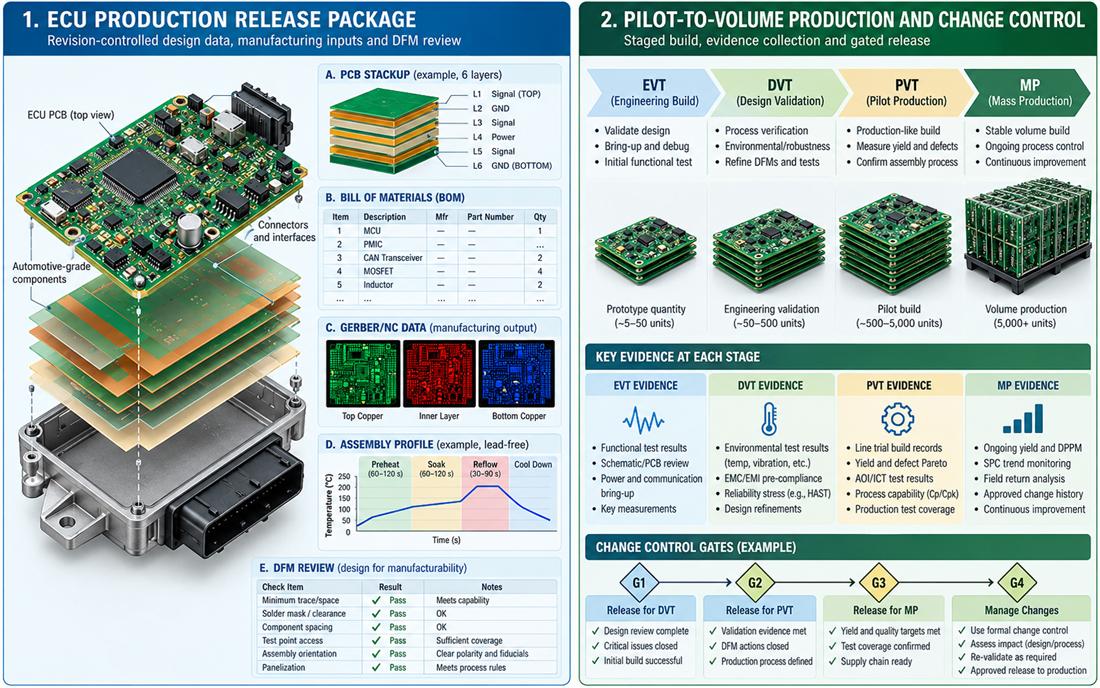
The release file should record the approved stackup, laminate construction, finished copper, impedance targets, drill and plating class, connector interface, solder-mask rule, thermal path, assembly profile, and acceptance method for critical features. Put the product requirement next to the board rule so a future engineer can tell whether a dimension is functional, mechanical, or inherited. The automotive PCB design package is complete only when those decisions are revisioned.
The program file should cross-reference automotive PCB design and signal integrity so design and sourcing see the same boundary. The released Automotive Electronics PCB page is an internal capability reference; the engineering decision remains in this article and the project file.
Make DFM responses measurable
Ask the fabricator to answer the actual geometry: minimum trace and space on the critical layers, registration at the connector or aperture, annular ring after plating, via-to-copper clearance, copper balance, panel rails, fiducials, and coupon placement. A generic “DFM approved” line does not say whether the supplier accepted the RF launch, sensor aperture, thermal pad, or housing edge. Use the PCB manufacturing review to close each question with an owner and date.
The handoff should name DFM review, multilayer PCB, and high-reliability PCB where those terms describe a controlled physical feature. The released Automotive Electronics PCB page is an internal capability reference; the engineering decision remains in this article and the project file.
Protect the loss, thermal, and service budget
Substitutions need a comparison across electrical footprint, dielectric and copper behavior, thermal resistance, mechanical envelope, plating, and service force. For Automotive Electronics PCB, a lower-cost or faster component can move the loss, phase, noise, heat, or connector datum enough to reopen the risk. Keep the high-reliability PCB and PCB assembly change records on the same change number. Keep RF PCB beside the drawing revision and assign thermal management PCB as the verification owner. The released Automotive Electronics PCB page is an internal capability reference; the engineering decision remains in this article and the project file.
Use staged evidence for pilot and volume
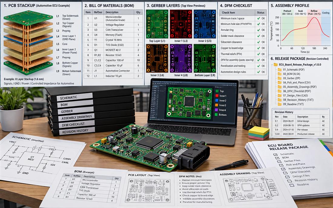
Separate prototype learning from production acceptance. Early builds may use an engineering range while the volume gate uses the released tolerance and sample plan. Define which checks are dimensional, coupon-based, visual, environmental, or functional; label typical values and design targets; and call a result measured only when the method, condition, and sample are retained. This makes the program status honest without weakening the engineering decision. The traveller can connect via design with surface finish PCB and preserve evidence for the next lot.
The released Automotive Electronics PCB page is an internal capability reference; the engineering decision remains in this article and the project file.
Close the supplier handoff on one revision
Before volume release, compare Gerber or ODB++, stackup, BOM, drawing, assembly program, inspection plan, material certificate, and change log. Confirm that the vehicle, mechanical, RF, fabricator, and assembler teams use the same revision. A board that is electrically correct but built from mixed revisions is not released. The final handoff should make the critical geometry and its verification method impossible to overlook. Before sign-off, confirm turnkey PCB assembly and PCB materials use the same revision and acceptance method.
Release checklist for the next vehicle build
- State the vehicle interface, operating band, and environmental boundary for Automotive Electronics PCB.
- Identify the controlled material construction, copper profile, and pressed dielectric tolerance.
- Show the signal and return path through connectors, vias, shields, planes, and housing datums.
- Tie fabrication and assembly checks to a revisioned drawing, coupon, or inspection record.
- Label typical values, design targets, engineering ranges, and measured values separately.
- Record the owner and closure evidence for each open RF, thermal, mechanical, and service risk.
Sources: Analog Devices RF and mixed-signal PCB layout guidance; Rogers automotive hybrid-multilayer design guidance; Würth Elektronik signal-integrity notes for internal connectors; and Qorvo front-end integration guidance. These authoritative engineering references inform the reasoning; no external link is inserted into the article and no customer measurement, certification, or simulation result is implied without retained project evidence.
