
ADAS PCB assembly release begins by treating heat, solder, cleaning, and mechanical force as RF variables. An RF board can leave fabrication within drawing limits and still change during paste printing, reflow, shielding, cleaning, or mechanical assembly. That risk is amplified in camera, radar, and domain-controller electronics that must keep data paths deterministic while surviving automotive assembly and service constraints, where thermal gradients and connector force coexist with sensitive RF geometry.
This production-oriented article turns the ADAS PCB assembly flow into a set of controllable variables, with special attention to warpage, solder volume, thermal paths, contamination, and inspection evidence.
Use the ADAS PCB release as a controlled engineering object: the board, stackup, fabrication note, assembly recipe, and verification record must describe the same physical path. The guidance below is intentionally practical; it separates a design target from a supplier typical value and keeps any inference visible.

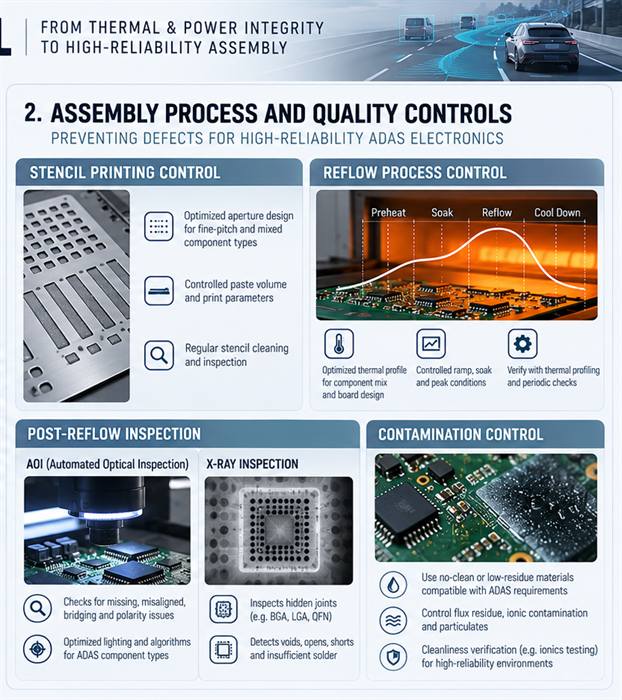
Table of Contents
ADAS PCB — Map heat and force before the first build
Mark the power devices, thermal vias, connector zones, thin edges, and antenna apertures on the assembly drawing. A large exposed pad can pull a board locally during reflow if copper and paste are unbalanced. A stiffener or shield frame can also introduce force after cooling. For ADAS PCB, simulate or reason through the thermal path from component to copper, dielectric, metal carrier, and enclosure; do not assume that a thicker copper plane automatically improves the joint. The result should be a placement and support plan that the contract manufacturer can follow. The project file should cross-reference PCB manufacturing and PCB assembly so the same constraint is visible to both design and sourcing. The controlled release record for this section is ADAS PCB; use the linked page as the internal capability reference while the article supplies the engineering decision.Control paste and reflow as RF variables
Paste volume changes pad height, connector coplanarity, and the amount of solder that can wick toward a launch. Define stencil aperture reductions for large pads, print inspection limits, soak and peak ranges, and the number of allowed reflow passes. The PCB assembly release should identify components that must not be reworked with a hot-air nozzle near the RF path. If the laminate supplier provides a profile window, treat it as a process constraint, not a suggestion. A practical handoff also names high-reliability PCB, signal integrity, and DFM review where those terms describe the physical feature being released. The controlled release record for this section is ADAS PCB; use the linked page as the internal capability reference while the article supplies the engineering decision.
Keep the surface clean without damaging the interface
Flux residues, ionic contamination, and aggressive cleaning can alter high-impedance nodes, adhesive bonds, or connector contact surfaces. Choose the cleaning method with the laminate, solder mask, shield, and conformal-coating plan in mind. Inspect under the connector and around via fences, not only the component side. For ADAS PCB, document whether the board is no-clean, aqueous-cleaned, or solvent-cleaned and define the acceptance evidence. A process that is electrically quiet in one lot can become unreliable when the chemistry, brush pressure, or drying time changes. Keep RF front-end PCB beside the drawing revision, and use thermal management PCB for the verification owner rather than leaving the requirement in email. The controlled release record for this section is ADAS PCB; use the linked page as the internal capability reference while the article supplies the engineering decision.Inspect the features that carry the RF risk
AOI can find missing parts and solder bridges, but it cannot prove that an internal return via is plated or that a connector launch is seated at the correct height. Pair AOI with X-ray, cross-section samples, coplanarity checks, and a functional RF screen selected for the real failure mode. The PCB manufacturing record should connect the board revision to the inspection plan so a project manager can trace a defect to a lot and process step. The manufacturing traveller can then connect via-in-pad PCB with multilayer PCB and preserve evidence for the next lot. The controlled release record for this section is ADAS PCB; use the linked page as the internal capability reference while the article supplies the engineering decision.
Release evidence instead of a pass label
For each pilot lot, retain stencil revision, paste lot, oven profile, inspection records, rework log, and the disposition of any RF-related defect. A simple “passed assembly” label hides whether the same issue was reworked three times. Use the high-reliability PCB requirements as a checklist for what must be preserved, then connect the evidence to the product risk review. Before sign-off, confirm PCB materials and RF PCB design are linked to the same revision and acceptance method.Release checklist for the next build
- State the operating band, enclosure state, and environmental boundary for ADAS PCB.
- Identify the controlled material construction, copper profile, and pressed dielectric tolerance.
- Show the complete signal and return path through connectors, vias, shields, and planes.
- Tie fabrication and assembly checks to a revisioned drawing, coupon, or inspection record.
- Label typical values, design targets, engineering ranges, and measured values separately.
- Record the owner and closure evidence for every open RF, thermal, and mechanical risk.
