
ADAS PCB launch design begins with a complete three-dimensional signal and return path. The boundary between a board and a connector, coax, antenna, or shield is where a clean schematic becomes a three-dimensional electromagnetic problem. In camera, radar, and domain-controller electronics that must keep data paths deterministic while surviving automotive assembly and service constraints, that boundary can set the usable bandwidth and the repeatability of every unit.
This guide focuses on the ADAS PCB transition itself: how to define the reference plane, shape the launch, provide a low-inductance return, and give manufacturing a geometry that can actually be inspected.
Use the ADAS PCB release as a controlled engineering object: the board, stackup, fabrication note, assembly recipe, and verification record must describe the same physical path. The guidance below is intentionally practical; it separates a design target from a supplier typical value and keeps any inference visible.
Table of Contents
ADAS PCB — Define the reference before routing
Name the signal reference at the interface: top-layer coplanar waveguide, stripline, microstrip, or an antenna feed with a defined ground aperture. Then show the return current path through the connector body and nearby vias. For ADAS PCB, the first reference plane should not disappear under a pad field without an intentional bridge. A connector drawing that gives only pin pitch and mechanical keep-out leaves the RF team to guess the electrical boundary.
Put the launch cross-section, pad, antipad, and via-fence intent on the PCB drawing.
The project file should cross-reference RF PCB design and controlled impedance PCB so the same constraint is visible to both design and sourcing. The controlled release record for this section is ADAS PCB; use the linked page as the internal capability reference while the article supplies the engineering decision.
Tune the geometry that the fab can hold
A transition is only repeatable when its critical dimensions have a process owner. Specify finished hole, capture-pad diameter, antipad diameter, copper-to-edge clearance, solder-mask opening, and ground-via pitch as controlled dimensions or approved ranges. Do not hide all tolerances in a generic class. The PCB design package should show which dimensions affect impedance and which are mechanical. If the design uses a press-fit or edge connector, include plating and wear constraints in the same review.
A practical handoff also names PCB manufacturing, PCB assembly, and high-reliability PCB where those terms describe the physical feature being released. The controlled release record for this section is ADAS PCB; use the linked page as the internal capability reference while the article supplies the engineering decision.

Use a via fence as a current-control tool
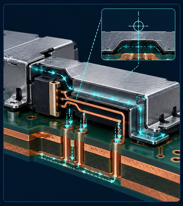
Ground vias beside the launch are not decoration. Their pitch, distance from the signal, connection to the reference planes, and drill aspect ratio define how well they contain the return field. For ADAS PCB, the fence should continue through the connector keep-out where the enclosure permits, then transition into the product ground strategy without a discontinuity. Avoid a fence that ends at a plane void or leaves a row of thermal vias to carry the RF return by accident.
A board-level shield or gasket also needs a continuous path; otherwise the mechanical feature becomes a slot antenna.
Keep signal integrity beside the drawing revision, and use DFM review for the verification owner rather than leaving the requirement in email. The controlled release record for this section is ADAS PCB; use the linked page as the internal capability reference while the article supplies the engineering decision.
Plan inspection and rework limits
A launch can be electrically wrong even when the board is visually acceptable. Add X-ray or cross-section checks for the critical via and plated interface, and define what rework is allowed near the RF path. Replacing a connector may lift a pad or change solder volume; a repair instruction must identify the acceptable condition, cleaning method, and post-rework verification. Use the PCB assembly process window rather than relying on a generic solder profile.
The manufacturing traveller can then connect RF front-end PCB with thermal management PCB and preserve evidence for the next lot. The controlled release record for this section is ADAS PCB; use the linked page as the internal capability reference while the article supplies the engineering decision.
Release the interface as a controlled subassembly
The project package should contain the connector part number, board stackup revision, launch drawing, return-via rule, torque or mating instruction, and the fixture used for correlation. When a supplier proposes a substitute connector, compare pad, shield, pin inductance, plating, and mating height—not just the footprint. This prevents an apparently minor component change from moving the antenna phase center or the router enclosure reference.
Before sign-off, confirm via-in-pad PCB and multilayer PCB are linked to the same revision and acceptance method.
Release checklist for the next build
- State the operating band, enclosure state, and environmental boundary for ADAS PCB.
- Identify the controlled material construction, copper profile, and pressed dielectric tolerance.
- Show the complete signal and return path through connectors, vias, shields, and planes.
- Tie fabrication and assembly checks to a revisioned drawing, coupon, or inspection record.
- Label typical values, design targets, engineering ranges, and measured values separately.
- Record the owner and closure evidence for every open RF, thermal, and mechanical risk.
Sources: Analog Devices mixed-signal PCB guidance, Qorvo RF front-end material, Würth high-speed interconnect examples, and Rogers thermal simulation guidance. These references inform the engineering reasoning; the article does not represent a customer measurement, a certification claim, or a simulated result unless the stated project evidence exists.
