
ADAS PCB stackup release begins by making every electromagnetic and manufacturing assumption visible. Stackup discussions fail when the drawing lists layer names but not the electromagnetic and manufacturing assumptions behind them. In camera, radar, and domain-controller electronics that must keep data paths deterministic while surviving automotive assembly and service constraints, the board must carry RF energy, power current, high-speed digital edges, and mechanical loads at the same time.
This article treats the ADAS PCB stackup as a release model: every dielectric, copper, via, and plane decision has a reason, a tolerance, and a verification method.
The objective is not to choose the most expensive laminate; it is to make the loss and variation budget visible early enough for the team to act.
Use the ADAS PCB release as a controlled engineering object: the board, stackup, fabrication note, assembly recipe, and verification record must describe the same physical path. The guidance below is intentionally practical; it separates a design target from a supplier typical value and keeps any inference visible.
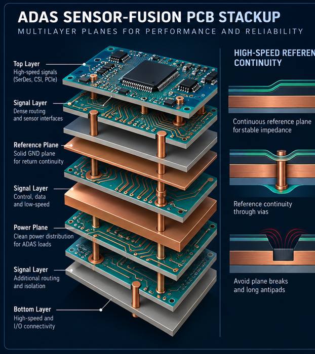
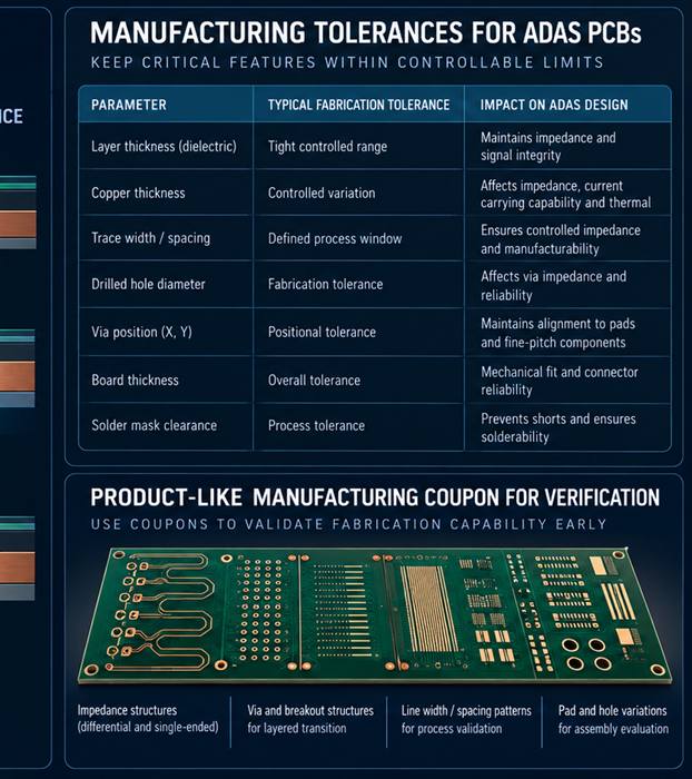
Table of Contents
ADAS PCB — Translate the system budget into board variables
Start with the frequency bands, route lengths, connector count, antenna aperture, and allowable link or phase margin. Then map them to board variables: dielectric thickness controls field confinement and impedance; copper profile affects conductor loss and etch sensitivity; surface finish changes the launch and solder interface; and via geometry limits the usable transition bandwidth. For ADAS PCB, the stackup review should show where the RF path changes layer, where the return plane is interrupted, and which digital aggressors share a reference. A stackup that looks balanced numerically can still be difficult to press if the resin flow and copper distribution are not compatible. The project file should cross-reference multilayer PCB and PCB materials so the same constraint is visible to both design and sourcing. The controlled release record for this section is ADAS PCB; use the linked page as the internal capability reference while the article supplies the engineering decision.Select construction by tolerance, not by name
A material family name is not a complete stackup specification. Record the intended resin content, pressed dielectric thickness, copper foil, glass style, and the supplier tolerance used for impedance calculation. Treat published Dk and loss values as typical or design-reference data unless the supplier gives a process-specific value. The safer handoff is a construction table with nominal thickness, allowed range, and the variable that will be checked on the coupon. Link the PCB materials choice to the RF PCB design rules so procurement cannot substitute a visually similar material without re-running the model. A practical handoff also names RF PCB design, controlled impedance PCB, and PCB manufacturing where those terms describe the physical feature being released. The controlled release record for this section is ADAS PCB; use the linked page as the internal capability reference while the article supplies the engineering decision.
Keep return current in the stackup conversation
At RF, the return path is part of the transmission line. A split plane, clearance slot, anti-pad cluster, or connector shield opening can force current into a longer loop. For ADAS PCB, review every layer change in a 3-D viewer and mark the nearest return vias. If an internal signal crosses a plane boundary, specify the bridge capacitor or alternate return strategy before routing is frozen. The layout should also consider the assembly state: solder mask, shield frame, thermal pad, and connector shell can change the local field. That is why a stackup cannot be signed off from a layer list alone. Keep PCB assembly beside the drawing revision, and use high-reliability PCB for the verification owner rather than leaving the requirement in email. The controlled release record for this section is ADAS PCB; use the linked page as the internal capability reference while the article supplies the engineering decision.Release the coupon with the product
The coupon should represent the critical line width, dielectric, copper, and transition used by the product. A coupon with a generous straight line may pass while the product launch fails. Define the coupon ID, measurement method, fixture, and acceptance band in the release package. Separate a design target from a measured value, and keep the measurement condition with the record. The PCB manufacturing traveller should point to the same construction revision that the designer used. The manufacturing traveller can then connect signal integrity with DFM review and preserve evidence for the next lot. The controlled release record for this section is ADAS PCB; use the linked page as the internal capability reference while the article supplies the engineering decision.
What the sourcing gate must prevent
The project manager should block three silent changes: an unapproved laminate substitution, a press-cycle change that moves dielectric thickness, and a copper foil change that alters loss or etch behavior. If schedule pressure requires a substitute, compare the new construction against the loss budget, impedance coupon, thermal expansion, and assembly profile before releasing it. A good stackup review leaves the supplier with measurable acceptance criteria rather than a brand-only instruction. Before sign-off, confirm RF front-end PCB and thermal management PCB are linked to the same revision and acceptance method.Release checklist for the next build
- State the operating band, enclosure state, and environmental boundary for ADAS PCB.
- Identify the controlled material construction, copper profile, and pressed dielectric tolerance.
- Show the complete signal and return path through connectors, vias, shields, and planes.
- Tie fabrication and assembly checks to a revisioned drawing, coupon, or inspection record.
- Label typical values, design targets, engineering ranges, and measured values separately.
- Record the owner and closure evidence for every open RF, thermal, and mechanical risk.
