
Automotive sensor modules combine a ceramic substrate with a connector, housing, adhesive, shield, and sometimes a high-frequency antenna. The Alumina PCB is stable, but the assembled module still sees vibration, thermal cycling, condensation, and connector loads. The project pain is often a fracture or intermittent contact at an edge feature that was reviewed only as a layout detail.
Treat the connector edge as a mechanical feature
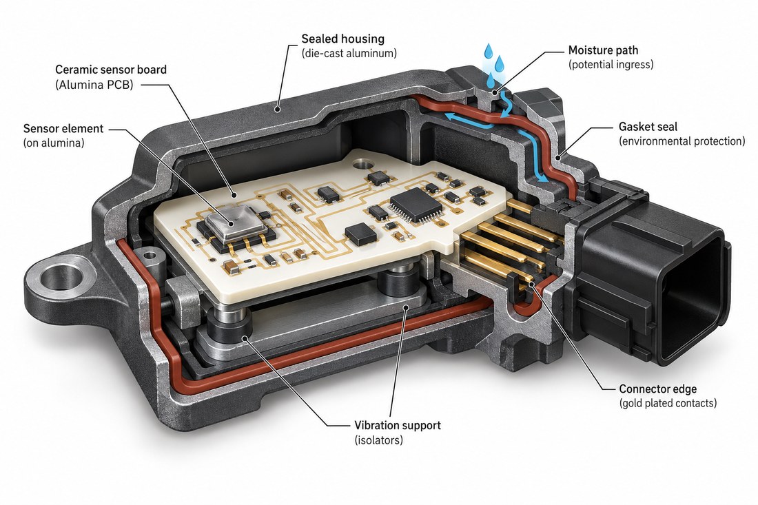
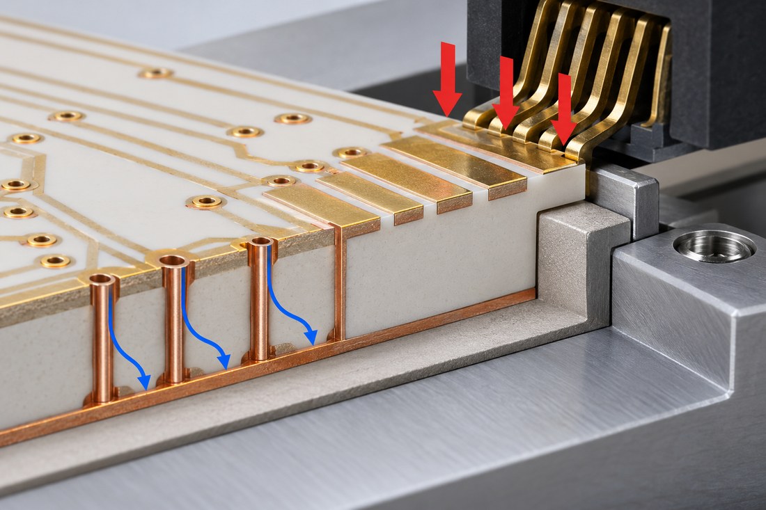
Define the connector datum, insertion force, board support, and housing stops before routing the sensor circuit. The Alumina PCB edge should have a clear unsupported length and a controlled metal termination. If the connector is press-fit, spring-loaded, or soldered, its force path must be visible in the mechanical drawing.
The RF PCB layout review should show the RF or sensor return around the connector, nearby mounting holes, and any shield spring. Keep a continuous path for the return current and avoid a slot that is created only to satisfy a housing rib.
Use supplier limits for the ceramic thickness, edge quality, and metallization. Do not treat a visual edge chip as cosmetic when it can grow under vibration or affect connector seating.
Close moisture and vibration interfaces
Map the moisture path through vent, gasket, adhesive, connector, and coating. The Alumina PCB substrate may absorb little water, but the module can still trap condensate at a metal or polymer interface. The controlled impedance reliability plan should identify the inspection location and the storage or bake condition.
For vibration, support the ceramic near corners and heavy components without creating a hard point that concentrates stress. Balance screw preload, gasket compression, and carrier flatness.
If a sensor line is high impedance, keep contamination and coating thickness outside the sensitive field unless the material has been qualified for that geometry.
Release a sensor-specific validation package
Define thermal cycling, vibration, connector cycling, and electrical or RF checks as separate evidence streams. A visual inspection alone cannot prove intermittent behavior, and a passing electrical test does not prove the mechanical margin.
The thermal management assembly package should record the adhesive cure, cleaning, connector installation, and final housing torque. A change in any of these can alter the stress or dielectric environment.
Close the design with an edge drawing, support map, moisture path, return path, and traceability checklist. That makes the sensor module easier to repeat across production lots.
An Alumina PCB in an automotive sensor is part of the mechanical package. Protect the connector edge, moisture boundary, return path, and support conditions together before validation.
Implementation note for this automotive sensor environment review: keep the engineering assumption visible at the point where it affects a drawing, a supplier quote, or an inspection record. Ask the design owner to identify the reference plane, interface datum, and acceptance method before the release is frozen. Ask manufacturing to return the proposed stack, panel, and process window rather than a generic capability statement. Ask assembly to identify the profile, cleaning, and support conditions that could move the RF or thermal result. This simple handoff prevents a typical material value from being mistaken for a guaranteed product result and gives the project team a clear action when an ECO changes the physical boundary.
Release note: keep the Alumina PCB edge connector, sealing approach, and vibration support defined before the automotive sensor build is quoted.
Sources: Panasonic MEGTRON technical material guidance; Rogers and Taconic high-frequency material data sheets where relevant; CeramTec ceramic substrate data; Analog Devices RF and mixed-signal layout guidance. Numerical values are treated as typical supplier values or engineering targets unless the released drawing defines a measured acceptance value.
Release note: confirm the Alumina PCB construction before the next ECO.
Release note: confirm the Alumina PCB construction before the next ECO.
Release note: confirm the Alumina PCB construction before the next ECO.
Release note: confirm the PCB manufacturing evidence before approval.
Release note: confirm the PCB assembly evidence before approval.
