
High-power microwave modules often fail at the thermal interface before they fail in the RF model. The finished RO5880 PCB must move heat away from the active device without disturbing the reference plane, launch geometry, or assembly datum. This engineering guide explains how to turn copper spreading and thermal-via decisions into a controlled design release without presenting unverified customer measurements.
Contents
Why RF thermal design needs a manufacturing plan
An RF power device creates a local heat source near controlled-impedance lines, ground transitions, and connector launches. If the copper path is too narrow, the device temperature rises. If the copper is spread into a sensitive RF field, the impedance model can change. A thermal RF PCB layout should therefore show heat-spreading zones and RF keep-outs on the same drawing.
For an RO5880 PCB, laminate data helps define the stackup model, but it does not prove a project-level temperature result. Mark which values are typical material information, which are design targets, and which require measurement on the approved assembly. This distinction prevents a nominal material property from being mistaken for a delivered thermal rating.
Build the copper-spreading path
Start with a device-centered copper island
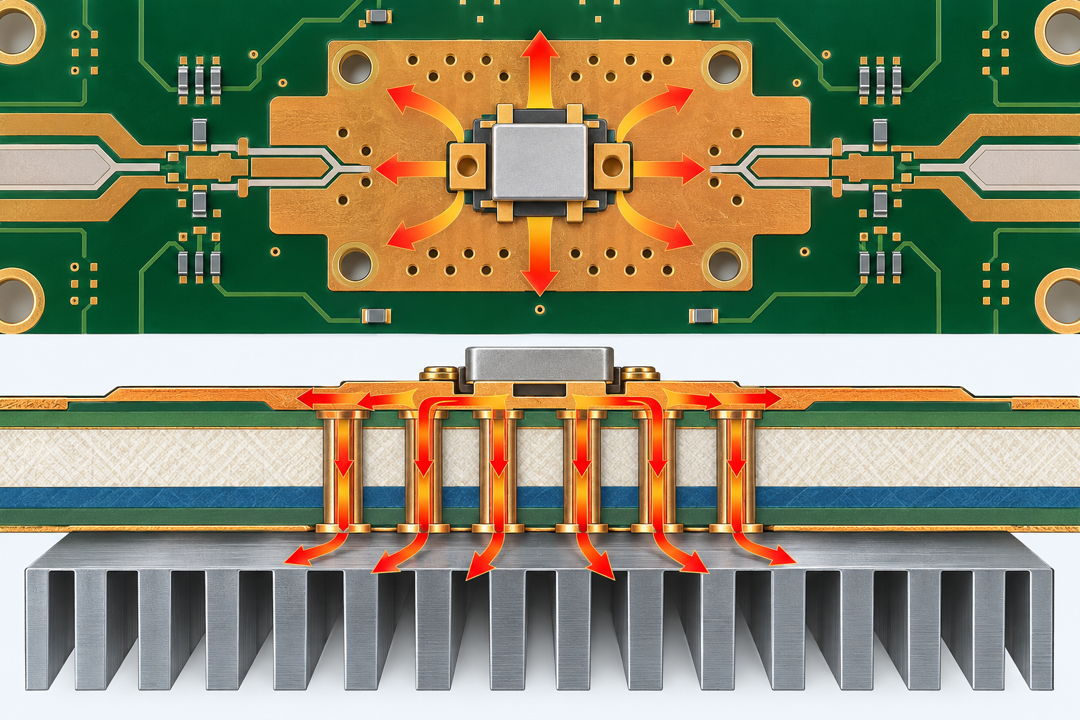
Use a device-centered copper island to collect heat, then widen the path toward the backside interface. Keep the island tied to the intended ground or thermal net, and document the copper thickness and finished surface requirement. Do not let a late RF fill change move the thermal boundary under a feed line. On a multilayer multilayer RF PCB, show the spreader on each participating layer so the lamination team can see where copper density changes.
Separate thermal and RF evidence
A thermal simulation can be a design target when its material inputs, boundary conditions, and device dissipation are recorded. It is not a measured result. If the project requires a thermal correlation, define the sensor location, fixture, power state, and acceptance method before the first build. Keep that record beside the stackup revision so the RO5880 PCB team can explain any later change.
Design the thermal-via field
Thermal vias reduce the vertical path from the device pad to the backside spreader, but the array must be manufacturable. Check drill diameter, aspect ratio, finished hole, plating, solder wicking risk, and the clearance to adjacent RF vias. If filled or capped vias are required, call out the process and inspection method instead of assuming a standard through-hole route.
Use a symmetric field when the package allows it. Symmetry helps distribute heat and reduces a local copper imbalance that can distort the panel. The PCB manufacturing review should compare the via field with the lamination construction, copper balance, and back-drill or sequential-build rules. Any change to the via count or pad diameter should trigger a thermal and RF review.
Balance thermal copper at panel level
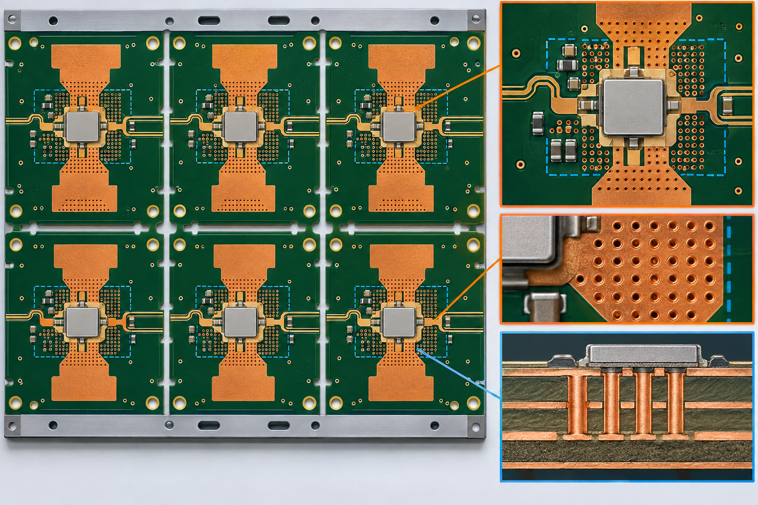
Large copper islands can pull the press stack, alter imaging behavior, or create a different etch response between center and edge boards. Add balancing copper in approved zones, but keep it outside antenna, feed, and connector keep-outs. The high-frequency PCB fabrication review should compare the electrical model with the panel drawing, not only with the individual board.
Record panel position, copper pattern revision, lamination cycle, material construction, drill program, and surface-finish route. A witness coupon or thermal cross-section can verify the intended layer order and plated-via structure. Those coupons are process evidence; they are not a substitute for a full product thermal qualification.
Verify the thermal path before release
Inspection should confirm the device pad, copper island, via field, backside interface, and any exposed-metal keep-out. Cross-sections can verify that the vias connect the intended layers and that plating is continuous. If a PCB assembly includes a metal carrier, heat spreader, or shield, define flatness, solder coverage, and attachment sequence so the thermal path is not left to operator interpretation.
When the project needs an electrical check, keep the RF coupon and thermal witness traceable to the same panel ID and material lot. Separate typical values, target values, and measured values in the report. This makes the RO5880 PCB release defensible without inventing a customer case or a test result.
RO5880 PCB thermal release checklist
- Show the device-centered spreader and RF keep-outs on the same drawing.
- Define thermal-via drill, plating, fill, cap, and inspection requirements.
- Review copper balance on every participating layer and at panel level.
- Document simulation assumptions separately from measured evidence.
- Trace coupons, panel position, lamination revision, and material lot.
- Freeze assembly attachment and backside-interface instructions.
KKPCB can review a RO5880 PCB thermal package for stackup, copper spreading, thermal vias, panel balance, and assembly handoff. The goal is a thermal path that remains visible and inspectable from layout through production.
Key takeaway
Thermal reliability on an RO5880 PCB comes from a coordinated copper path, manufacturable via field, balanced panel, and traceable inspection plan. Lock the thermal boundary before RF fill changes, keep targets separate from measurements, and give assembly a clear interface definition. That workflow helps a high-power module move from prototype to volume production with fewer surprises.
Sources: Rogers Corporation RT/duroid 5880 material information and fabrication guidance; IPC-TM-650 methods for printed-board dimensional and cross-section inspection; KKPCB internal high-frequency DFM capability notes. Values are typical or target references unless explicitly identified as measured.
