
Outdoor radar and microwave equipment can see humidity, temperature swings, and repeated handling before a board reaches final system test. For a PTFE-based laminate, the project risk is not only RF loss; it is whether the finished RO5880 PCB keeps its layer registration, connector datum, and antenna geometry through the approved process. This RO5880 PCB article turns that risk into a practical design-for-manufacturing checklist without implying unverified environmental results.
In this guide:
- RF datum and stackup control
- Panel registration and copper balance
- Environmental witness and dimensional checks
- Release checklist
Why dimensional stability is an RF design variable
A small shift in dielectric thickness or registration can move a feed line relative to its reference plane. At an array or connector, that shift can appear as phase or return-loss variation. A high-frequency PCB drawing should therefore identify the mechanical datums that protect the RF geometry, not just the finished outline.
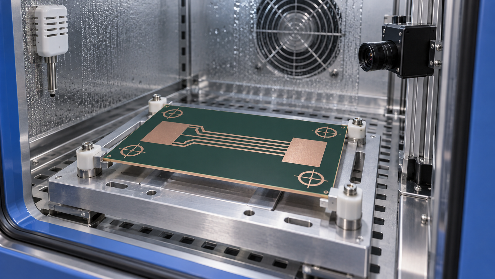
Separate typical material behavior from project evidence
Rogers publishes typical RT/duroid 5880 properties and processing guidance. Those references help define a model, but they do not replace a build-specific inspection plan. On a new RO5880 PCB, mark which values are typical material data, which are design targets, and which require measurement on the approved panel and lot.
RO5880 PCB RF datum through the stackup and panel
Each panel copy should preserve the same electrical datum and inspection relationship.
Use one master datum for RF apertures, connector launches, tooling holes, and inspection fiducials. Keep the datum visible from the individual board drawing through the panel drawing and assembly fixture. If the panel is mirrored or rotated, document the transformation so a registration review can compare equivalent features.
| Datum or feature | Risk if it moves | Control |
|---|---|---|
| RF aperture or feed | Phase and coupling shift | Tie the feed to the master datum and reference plane |
| Connector launch | Mechanical and electrical misalignment | Share tooling and assembly datums |
| Panel fiducial | Imaging or placement offset | Use representative fiducials on rails and board |
| Stackup reference | Dielectric spacing changes | Verify layer order and finished thickness by coupon |
Use copper balance without disturbing the RF field
Balanced copper helps the panel press and image consistently, but fill must stay outside antenna and sensitive feed keep-outs. A RF stackup review should show both copper-balance zones and RF exclusions. When a PCB manufacturing revision changes fill or rail geometry, recheck the registration and the electrical model.
Build an environmental and registration witness plan
An environmental witness plan can combine dimensional fiducials, cross-section coupons, and representative RF coupons. Measure before and after the approved conditioning sequence if the project requires environmental correlation. Keep the method, temperature or humidity range, dwell time, and fixture orientation in the test plan; do not substitute a generic claim of “outdoor qualified” for evidence.
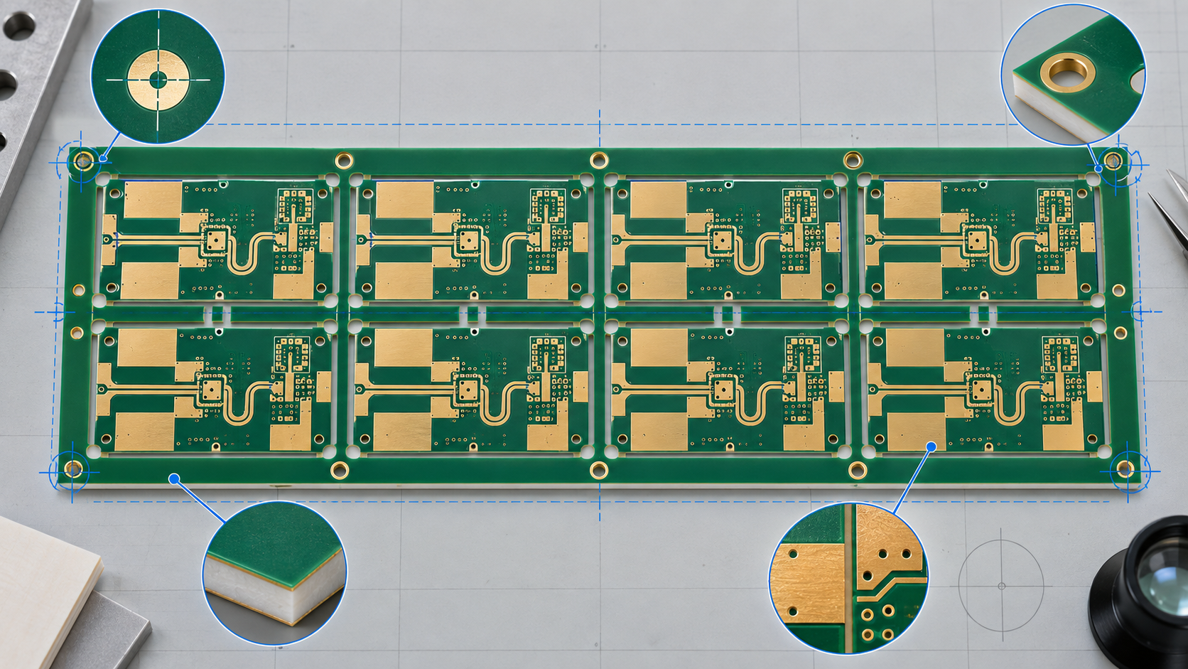
Correlate panel position and process revision
Record panel ID, lot, material construction, drill program, lamination revision, and surface-finish route with each witness. Compare center and edge locations when copper density or panel aspect ratio makes them different. If a feature shifts with panel position, review registration and copper balance before changing the RF geometry. This keeps the RO5880 PCB release focused on the real source of variation.
RO5880 PCB dimensional-control checklist
- Lock a master RF datum and show any mirrored panel copies.
- Identify fiducials, tooling holes, connector launches, and antenna keep-outs.
- Separate typical laminate data, design targets, and measured evidence.
- Review copper balance outside RF fields on every layer.
- Define cross-section and RF coupons with panel position and lot traceability.
- Document any environmental conditioning and its acceptance method.
KKPCB can review a multilayer RO5880 PCB package for stackup datums, panel registration, copper balance, and witness coverage. The goal is to expose dimensional risk while the drawing and process window can still be adjusted.
Key takeaway
A stable RO5880 PCB is built around a datum that survives design, panelization, lamination, and inspection. By linking fiducials and coupons to the RF geometry, teams can discuss environmental and registration risk with evidence instead of assumptions. The same RO5880 PCB manufacturing method supports prototype and volume builds: lock the datum, document the process, and verify the changed variable.
Questions to close before panel release
Ask whether the RF datum is shared by layout, tooling, and inspection; whether the stackup revision matches the material lot; whether copper fill is outside the antenna field; and whether the witness plan can identify a panel-position effect. If any answer is unknown, mark it as an open engineering action. A concise handoff is safer than an assumed tolerance, especially when an RO5880 PCB is moving from a prototype drawing to a repeatable production panel. Keep the responsible owner, due date, and evidence type with the action so a later revision does not erase the decision trail.
Sources: Rogers Corporation RT/duroid 5880 material information and fabrication guidance; IPC-TM-650 dimensional, registration, and environmental methods; KKPCB internal high-frequency DFM capability notes. Values are typical or target references unless explicitly identified as measured.
