
PTFE laminates deliver very low RF loss, but their mechanical behavior changes the way a via is drilled, desmeared, plated, and inspected. A robust RO5880 PCB release therefore treats via reliability as an electrical and manufacturing problem together. The goal is a repeatable transition that does not hide voids, barrel damage, or registration risk behind a low-loss material callout.
Why PTFE via fabrication needs a different handoff
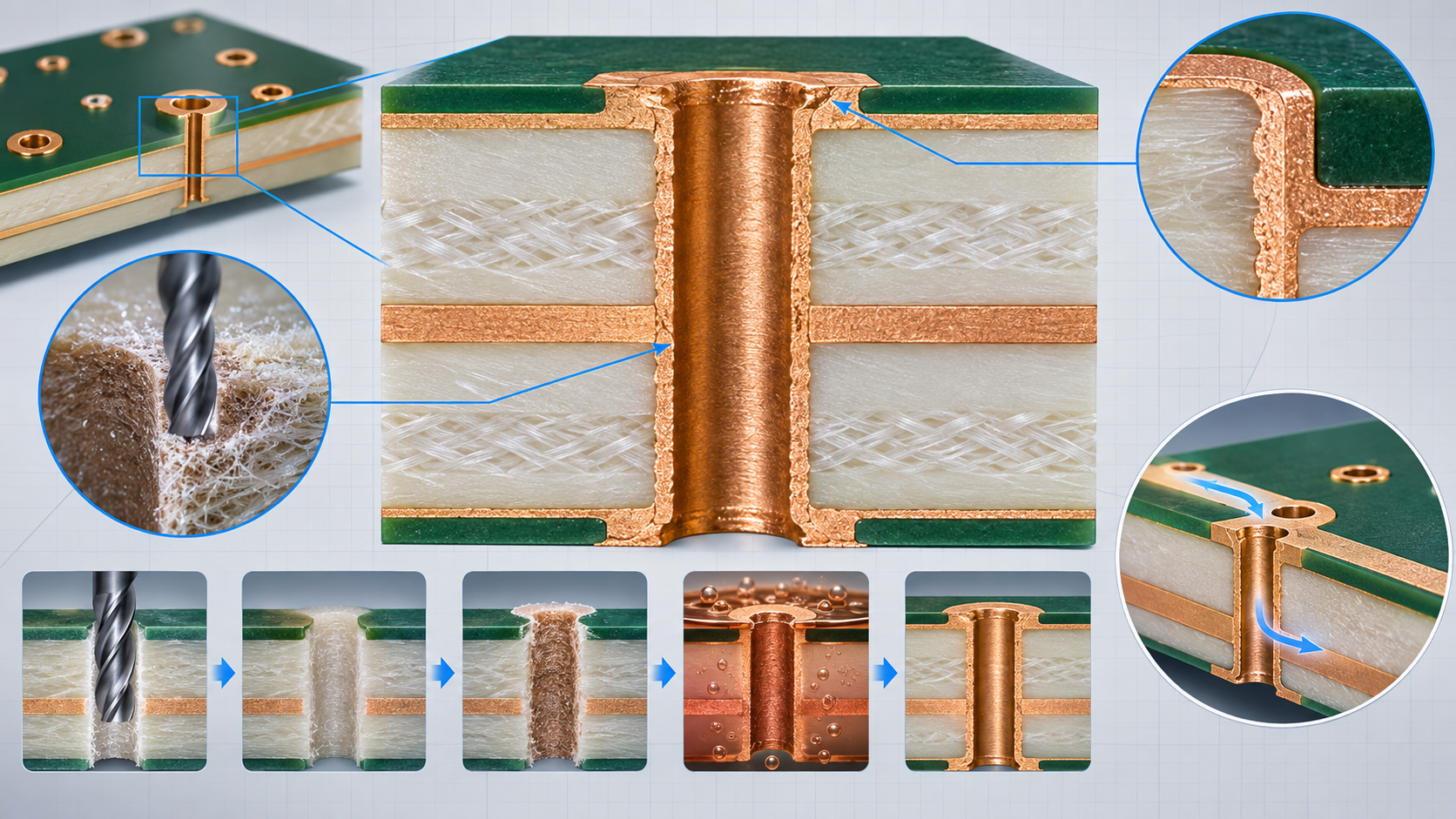
PTFE-based constructions can behave differently from standard epoxy/glass during drilling and copper preparation. Drill energy, tool wear, hole-wall conditioning, and plating adhesion all affect the finished barrel. For a high-frequency PCB, a damaged or poorly plated via can add loss, create a discontinuity, or open after thermal cycling. The drawing should identify the RF layer pair, via type, finished hole requirement, and inspection method before tooling begins.
Start with the finished transition
Define the pad, antipad, reference-plane clearance, and any back-drill or blind-via requirement from the RF model. On a new RO5880 PCB, record whether the design uses a plated through-hole, a controlled-depth blind via, or a mechanical transition between laminate sections. This prevents the fabricator from interpreting a generic drill table as permission to change the electrical geometry.
RO5880 PCB drilling, desmear, and copper preparation
A production RO5880 PCB process needs material-specific drill and copper preparation rules documented before release.
A PTFE via process needs a qualified sequence for drill entry, tool selection, hole-wall cleaning, and copper deposition. The exact recipe depends on the selected construction and supplier guidance; it should not be invented from an FR-4 default. Track drill count, tool condition, panel location, and the approved process revision. If a PCB manufacturing change alters the drill or preparation sequence, recheck the RF transition and coupon plan.
| Process stage | Failure mode | Engineering control |
|---|---|---|
| Drilling | Smear, burr, or wall damage | Use an approved tool and inspect representative holes |
| Hole-wall preparation | Weak copper adhesion | Qualify the cleaning and activation sequence for the material |
| Electroless copper | Coverage voids or thin seed | Track bath condition and coupon evidence |
| Electroplating | Uneven barrel build | Review current distribution and finished-hole requirements |
Keep the RF return path visible
Via fences and ground transitions are part of the RF circuit. A fence that is mechanically present but poorly registered can leave an inconsistent return path. An RF via design review should show the reference plane, antipad, neighboring copper, and the allowed drill wander. If a multilayer PCB uses mixed materials, review every transition rather than copying a via rule from a different laminate.
Use representative coupons and cross-sections
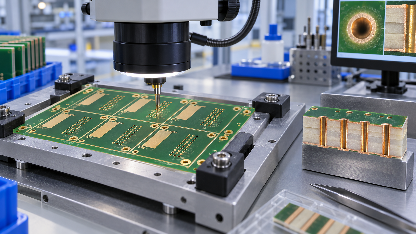
A useful RO5880 PCB via coupon matches the RF layer pair, pad size, hole type, copper weight, and plating route of the product. Place witnesses where panel copper distribution and drilling orientation are representative. Cross-section work can confirm layer order, barrel continuity, copper coverage, and registration at the coupon location, but it cannot prove every product via is identical. Label the evidence as a target, typical process value, or measured result.
Connect via evidence to RF acceptance
For a controlled impedance PCB, keep the via coupon result with the panel ID, stackup revision, drilling program, and finish route. This makes it easier to separate a layout issue from a drilling or plating excursion. Do not label a conceptual diagram as a measured case study or imply customer results that are not documented.
RO5880 PCB release checklist
- Define finished via, pad, antipad, and reference-plane requirements.
- Identify PTFE construction, drill type, and approved preparation sequence.
- State the inspection method and representative coupon geometry.
- Review via-fence registration and return-current continuity.
- Track tool condition, panel location, lot, and process revision.
- Separate material typicals, design targets, and measured acceptance data.
KKPCB can review an RO5880 PCB manufacturing package for drill strategy, via coupons, plating controls, and RF transition clarity. The review is most useful before the drill file is released, while the electrical and process datums can still be aligned.
Key takeaway
A reliable RO5880 PCB via is created by coordinating the RF transition with the PTFE drilling and plating process. The same RO5880 PCB discipline applies from prototype to volume: document the finished geometry, qualify the material-specific process, and use representative coupons to make reliability evidence traceable.
Sources: Rogers Corporation RT/duroid 5880 product information and fabrication guidance; IPC-TM-650 hole-wall, plating, dimensional, and impedance methods; KKPCB internal RF via and high-frequency manufacturing capability notes. Numerical values are typical or target references unless explicitly identified as measured.
