
Why Multilayer PCBs Became Standard
As electronic systems evolved from simple circuits to highly integrated platforms, single-layer and double-layer PCBs quickly reached their limits. Multilayer PCBs—typically defined as boards with 4 or more layers—became the standard solution for handling increased complexity.
By stacking multiple conductive and insulating layers, engineers can:
- Route more signals within limited space
- Separate signal, power, and ground planes
- Improve overall electrical performance
Today, multilayer PCBs are used in almost every advanced application, from consumer electronics to high-speed computing and industrial systems.
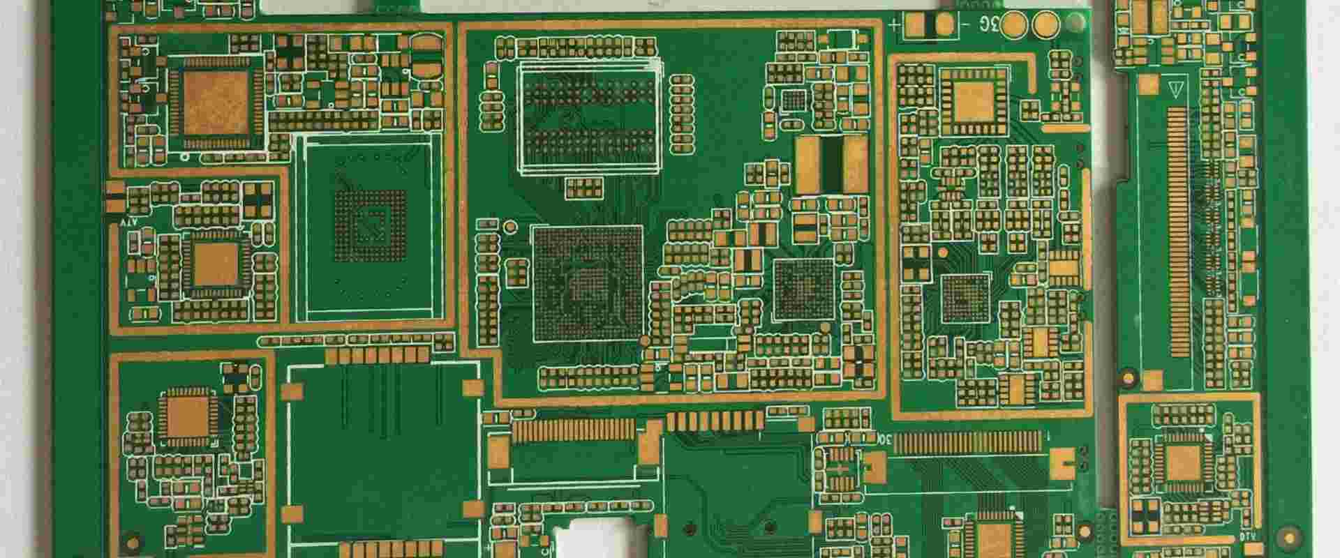
Stack-Up Logic: The Foundation of Performance
The real value of a multilayer PCB lies in its stack-up design. A well-structured stack-up determines both electrical performance and manufacturability.
Key principles include:
- Symmetry:
Balanced layer structures reduce warpage during fabrication and assembly - Dedicated Planes:
Separate power and ground planes improve signal return paths and reduce noise - Layer Function Assignment:
Different layers are allocated for high-speed signals, low-speed signals, RF, or power - Dielectric Thickness Control:
Critical for impedance control and signal timing
A typical multilayer stack-up is not just a physical structure—it is a designed electrical environment.
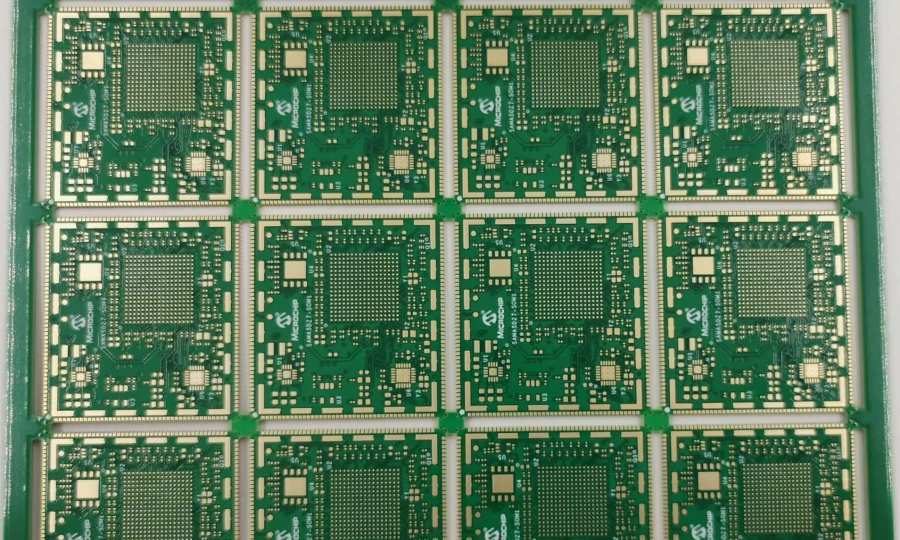
Electrical Performance: SI and PI Benefits
Multilayer PCBs significantly improve both Signal Integrity (SI) and Power Integrity (PI):
- Reduced Crosstalk:
Ground planes between signal layers act as shields - Controlled Impedance:
Stable dielectric thickness allows precise impedance design - Improved Return Paths:
Continuous ground planes reduce loop area and noise - Stable Power Delivery:
Power planes provide low-impedance paths for current distribution - Support for High-Speed Signals:
Essential for interfaces like DDR, PCIe, and high-speed serial links
These advantages make multilayer PCBs essential for modern high-speed and high-frequency systems.
Design Trade-Offs
While multilayer PCBs provide clear benefits, they also introduce trade-offs:
- Cost vs Layer Count:
More layers increase material and manufacturing cost - Complexity vs Manufacturability:
Higher layer counts require tighter process control - Thermal Management:
Dense multilayer structures can trap heat if not properly designed - Signal Layer vs Plane Balance:
Too many signal layers without sufficient planes can degrade performance
A key engineering principle:
More layers do not automatically mean better performance—only optimized layers do.
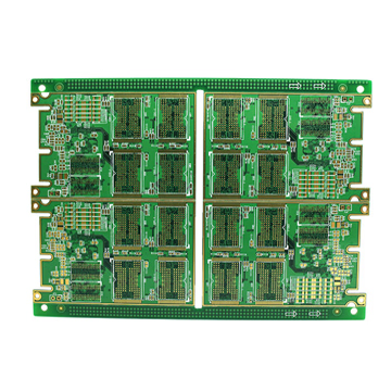
When Should You Increase Layer Count?
Deciding to move from a lower-layer design to a higher-layer PCB should be based on clear needs:
Increase layer count when:
- Routing becomes congested
- High-speed signals require better isolation
- Power delivery needs improved stability
- Multiple subsystems must be separated
Avoid unnecessary layers when:
- Design requirements can be met with fewer layers
- Cost constraints are critical
- Signal speeds are relatively low
A well-optimized 6-layer board can often outperform a poorly designed 10-layer board.
Final Thoughts
Multilayer PCBs are the backbone of modern electronics, enabling designers to balance density, performance, and scalability.
Their true value lies not in the number of layers, but in how those layers are structured, assigned, and optimized.
At KKPCB, we support multilayer PCB development with stack-up optimization, impedance control, and advanced manufacturing processes, helping customers achieve the best balance between performance, reliability, and cost.
