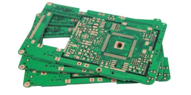
In modern digital electronics, ensuring that circuits function correctly before mass production is essential. Logic Test PCBs are specialized printed circuit boards designed to validate the functionality of digital systems, identify defects, and verify signal logic.
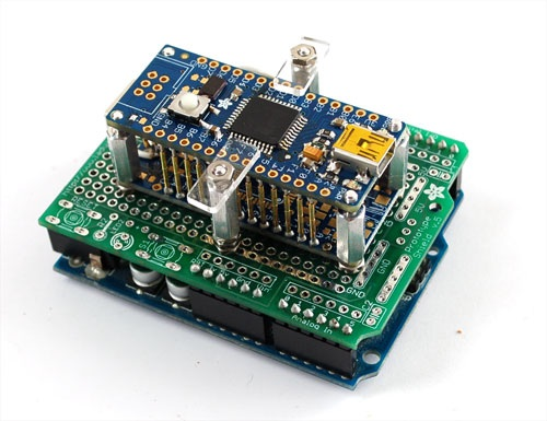
From microcontrollers and FPGAs to high-speed memory and communication modules, Logic Test PCBs play a critical role in the development and production of reliable electronic devices.
What is a Logic Test PCB?
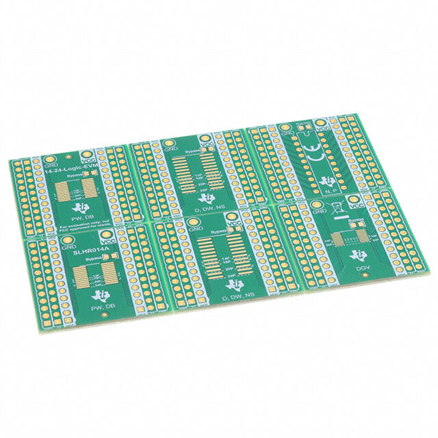
A Logic Test PCB is a circuit board used for functional verification and digital testing of electronic devices. These PCBs allow engineers to check signal integrity, logic states, timing sequences, and system responses under controlled conditions.
Common uses include:
-
Validating microcontroller or FPGA circuits
-
Testing memory modules or interface boards
-
Performing automated functional testing for production lines
-
Debugging timing, logic errors, or power sequencing issues
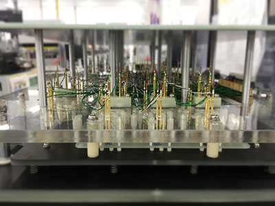
Logic Test PCBs can integrate with test fixtures, connectors, and automated test equipment (ATE) to streamline the verification process.
Key Features of Logic Test PCBs
Designing an effective Logic Test PCB requires attention to several key factors:
Accurate Signal Routing
Digital signals, especially at high speeds, require precise trace routing to maintain timing and prevent interference. Controlled impedance and minimal crosstalk are essential for accurate testing.
Test Point Accessibility
Logic Test PCBs are designed with accessible test points or headers, enabling engineers to connect measurement tools like oscilloscopes, logic analyzers, or automated test systems.
Thermal and Electrical Stability
Even though most logic testing doesn’t involve extreme temperatures, boards must remain stable under prolonged operation or high-frequency switching to prevent false readings.
Compatibility with Automated Testing
Logic Test PCBs are often integrated into production-line functional test setups, ensuring devices meet quality standards before shipment.
Manufacturing Considerations
Producing Logic Test PCBs requires high-quality materials and precise fabrication processes:
-
High-Precision Copper Traces: Ensure consistent signal performance.
-
Stable PCB Substrate: Prevents warping or dimensional changes.
-
Quality Surface Finishes: ENIG, OSP, or HASL finishes improve solder reliability and probe contact.
-
Controlled Impedance (Optional): For high-speed digital circuits, impedance control maintains signal integrity.
Attention to these factors ensures reliable testing and accurate functional verification.
Applications of Logic Test PCBs
Logic Test PCBs are widely used across industries for digital circuit verification:
-
Embedded Systems: Microcontrollers, SoCs, and interface boards
-
Consumer Electronics: Smartphones, tablets, and wearables
-
Industrial Automation: PLCs, motor controllers, and control boards
-
High-Speed Memory and Communication Modules: DDR, PCIe, and Ethernet devices
By detecting design flaws or production defects early, Logic Test PCBs help reduce failure rates and increase product reliability.
Choosing the Right Manufacturer
Selecting an experienced PCB manufacturer ensures Logic Test PCBs meet functional testing requirements. Look for:
-
Expertise in digital and high-speed PCB design
-
Precision fabrication and QA processes
-
Flexibility for custom test point placement and layouts
-
Experience supporting automated testing and production verification
Partnering with a skilled manufacturer helps accelerate development and improves testing accuracy.
Conclusion
Logic Test PCBs are essential tools for validating digital circuits and ensuring the functional integrity of electronic devices. By enabling accurate testing of logic states, timing, and signal behavior, these PCBs help engineers deliver reliable products and reduce production failures.
Investing in high-quality Logic Test PCB design and manufacturing is a critical step toward achieving robust, high-performance electronics.
