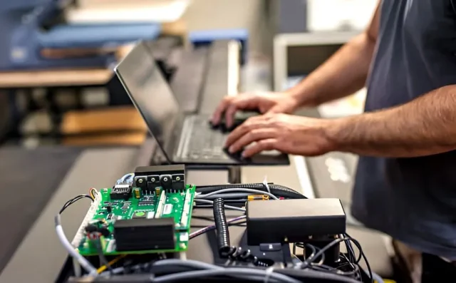
As wireless communication technologies continue to evolve, accurate testing of radio frequency circuits has become critical for product reliability and performance. From IoT modules and satellite communication equipment to radar and 5G devices, RF testing ensures that systems operate correctly under real-world signal conditions.
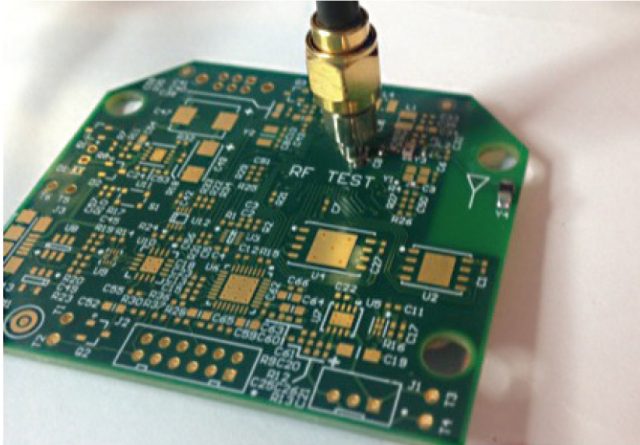
One essential tool in this process is the RF Test PCB, a specialized printed circuit board designed to evaluate and measure RF components, circuits, and modules. Unlike standard PCBs, RF Test PCBs must meet strict requirements for impedance control, signal integrity, and high-frequency performance.
This article explores what RF Test PCBs are, their design requirements, and the manufacturing considerations necessary for reliable RF testing.
What is an RF Test PCB?
An RF Test PCB is a circuit board specifically designed to test and evaluate radio-frequency components or systems. These boards are commonly used in the development and validation stages of RF devices.
Typical applications include:
-
Testing RF modules and antennas
-
Evaluating microwave circuits
-
Measuring signal integrity and insertion loss
-
Characterizing RF amplifiers, filters, and mixers
-
Verifying impedance matching networks
RF Test PCBs often include connectors such as SMA, MMCX, or SMP interfaces, allowing engineers to connect measurement equipment like spectrum analyzers, vector network analyzers (VNA), or signal generators.
Key Design Considerations for RF Test PCBs
Designing an RF Test PCB requires careful attention to several high-frequency design factors.
Controlled Impedance
Maintaining consistent impedance is essential in RF testing environments. Transmission lines such as microstrip or stripline must be precisely calculated to ensure 50-ohm impedance matching, minimizing signal reflections and measurement errors.
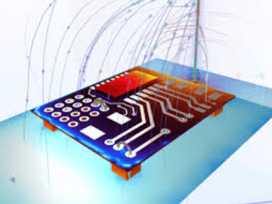
Signal Integrity
High-frequency signals are sensitive to discontinuities in PCB layout. Proper trace routing, smooth transitions, and minimized via usage help maintain signal integrity and reduce loss.
Grounding and Shielding
A stable ground plane is critical for RF testing. Designers typically use solid ground layers and via stitching to reduce electromagnetic interference (EMI) and maintain signal stability.
Connector Integration
RF connectors must be carefully integrated into the PCB layout. Improper connector placement can introduce impedance mismatches and degrade signal quality.
Short Signal Paths
RF signals suffer greater loss over long traces. Keeping signal paths short and direct helps preserve signal strength and improves measurement accuracy.
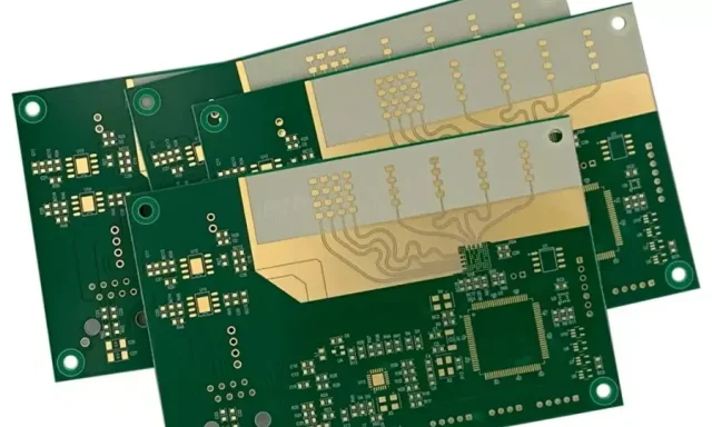
Materials Used for RF Test PCBs
High-frequency testing often requires specialized PCB materials with stable dielectric properties.
Common materials include:
-
Rogers laminates (RO4350B, RO4003C)
-
PTFE-based substrates
-
Taconic high-frequency materials
-
Ceramic-filled hydrocarbon laminates
These materials provide low dielectric loss, stable dielectric constant (Dk), and improved thermal performance compared with standard FR4.
Manufacturing Challenges of RF Test PCBs
Producing RF Test PCBs requires advanced fabrication capabilities and strict process control.
Key challenges include:
Precision impedance control
Even small variations in trace width or dielectric thickness can affect RF performance.
Low-loss material processing
High-frequency materials require specialized drilling, lamination, and surface treatment processes.
High-frequency surface finish compatibility
Surface finishes such as ENIG or immersion silver are commonly used to ensure reliable RF performance.
Tight tolerance fabrication
High-frequency PCBs often require tighter tolerances than conventional boards.
Applications of RF Test PCBs
RF Test PCBs are widely used in various advanced technology industries.
Common application areas include:
-
Wireless communication devices
-
IoT modules and gateways
-
Satellite communication equipment
-
Radar and aerospace systems
-
RF power amplifiers and filters
-
5G and microwave devices
These industries rely on RF Test PCBs to validate circuit performance before mass production.
Choosing the Right RF Test PCB Manufacturer
Because RF performance depends heavily on PCB quality, selecting an experienced manufacturer is crucial. A reliable PCB partner should offer:
-
Expertise in high-frequency PCB materials
-
Accurate impedance control capabilities
-
Advanced fabrication and inspection processes
-
Experience with RF and microwave PCB designs
Working with a manufacturer familiar with RF testing requirements can significantly improve development efficiency and testing accuracy.
Conclusion
RF Test PCBs play a critical role in the development and validation of high-frequency electronic systems. By ensuring accurate signal measurement and stable RF performance, these specialized PCBs help engineers optimize wireless and communication devices before they reach the market.
With the growing demand for IoT, satellite communication, and high-speed wireless technologies, the importance of high-quality RF Test PCB manufacturing will continue to increase.
