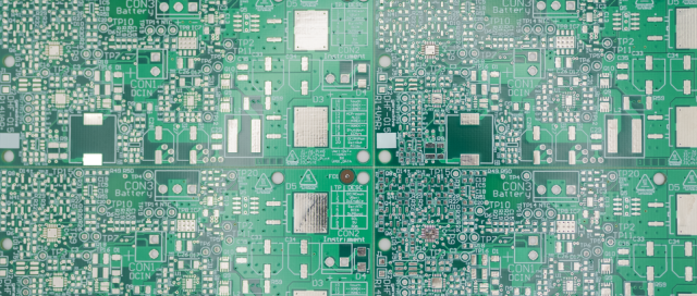
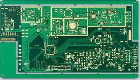
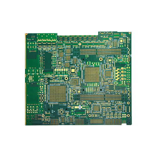
A Multilayer Test PCB is a specialized printed circuit board designed for testing, validation, and performance verification of electronic components, integrated circuits, and complex systems. Compared with standard PCBs, multilayer test boards incorporate multiple conductive layers to support high-density routing, signal integrity analysis, and accurate electrical testing.
With the rapid development of modern electronics such as telecommunications equipment, semiconductor devices, automotive electronics, and high-speed computing systems, multilayer test PCBs have become essential tools in both product development and quality assurance processes.
These boards allow engineers to simulate real operating environments, verify circuit performance, and detect potential issues before mass production.
What Is a Multilayer Test PCB?
A multilayer test PCB consists of three or more conductive copper layers laminated together with insulating materials. These layers are interconnected through plated vias, enabling complex circuit routing and testing structures.
Unlike standard multilayer PCBs used in final products, test PCBs are designed specifically for:
-
Electrical performance testing
-
Functional verification
-
Signal integrity evaluation
-
Component validation
-
Reliability testing
Multilayer structures enable engineers to replicate actual product conditions, especially in high-speed or high-frequency designs.
Key Design Considerations
Designing a multilayer test PCB requires careful attention to several technical factors.
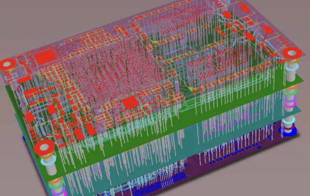
Layer Stackup Planning
A proper layer stackup ensures signal integrity and electromagnetic compatibility. Typical multilayer test boards may include:
-
Signal layers
-
Power planes
-
Ground planes
-
Controlled impedance routing layers
Balanced stackups help reduce noise and maintain stable electrical performance.
Signal Integrity
High-speed signals require controlled impedance traces, proper return paths, and minimized crosstalk. Designers often integrate:
-
Differential pair routing
-
Ground shielding
-
Short signal paths
These features help ensure accurate testing results.
Thermal Management
Testing environments sometimes involve high current or power loads. Thermal vias, copper pours, and heat dissipation areas help maintain board reliability during testing.
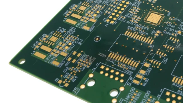
Test Point Accessibility
Multilayer test boards often include numerous test pads and probe points to allow measurement equipment such as oscilloscopes, logic analyzers, and automated test systems to access signals easily.
Manufacturing Process
The manufacturing process for multilayer test PCBs is similar to that of standard multilayer boards but may involve additional precision requirements.
Material Preparation
Common base materials include:
-
FR-4
-
High-frequency laminates
-
Low-loss dielectric materials
The material selection depends on the testing requirements.
Inner Layer Fabrication
Each inner copper layer is etched to form the required circuitry before lamination.
Lamination
Multiple layers are pressed together under controlled temperature and pressure to create a unified board structure.
Drilling and Via Formation
Mechanical drilling or laser drilling is used to create vias that electrically connect different layers.
Surface Finishing
Surface finishes such as ENIG, HASL, or immersion silver are applied to ensure good solderability and reliable test contact.
Applications of Multilayer Test PCB
Multilayer test boards are widely used across various high-tech industries.
Semiconductor Testing
Used for testing IC packages, chip validation, and performance characterization.
High-Speed Digital Systems
Essential for verifying signal integrity in high-speed computing and networking equipment.
Telecommunications Equipment
Used in testing RF modules, base station hardware, and communication devices.
Automotive Electronics
Supports testing of advanced driver assistance systems (ADAS), sensors, and control modules.
Automated Test Equipment (ATE)
Multilayer test PCBs are often integrated into ATE systems for large-scale product testing.
Advantages of Multilayer Test PCBs
Using multilayer structures for testing provides several benefits:
-
Higher circuit density
-
Improved signal integrity
-
Better power distribution
-
More realistic system simulation
-
Enhanced testing accuracy
These advantages make multilayer test PCBs an essential component in modern electronics development.
Conclusion
As electronic systems continue to grow in complexity, multilayer test PCBs play a crucial role in ensuring product performance, reliability, and quality. By providing high-density routing, controlled impedance environments, and extensive testing capabilities, these boards enable engineers to validate designs efficiently before production.
For companies involved in advanced electronics manufacturing, investing in high-quality multilayer test PCBs can significantly improve development efficiency and reduce potential design risks.
