What Is a Heavy Copper PCB?
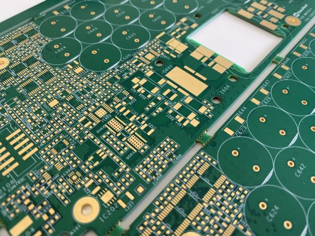
A Heavy Copper PCB is a printed circuit board manufactured with thick copper layers, typically 3 oz/ft² and above. In some high-power applications, copper thickness can reach 10 oz, 20 oz, or even more depending on current requirements.
Unlike standard 1 oz copper PCBs, heavy copper boards are designed to handle high current loads, improve heat dissipation, and enhance mechanical durability.
Why Copper Thickness Matters
Copper thickness directly affects:
-
Current carrying capacity
-
Thermal conductivity
-
Voltage drop performance
-
Mechanical strength
Thicker copper traces reduce resistance, allowing higher current flow while minimizing heat generation.
For high-power systems, proper copper thickness selection is critical to ensure long-term reliability.
Key Advantages of Heavy Copper PCB
1. High Current Handling
Heavy copper PCBs can support:
-
High current power rails
-
Motor driver circuits
-
Battery management systems
-
Power converters
They reduce overheating risks under heavy load.
2. Improved Thermal Management
Thick copper acts as a heat spreader, distributing heat more evenly across the board.
Combined with:
-
Thermal vias
-
Large copper planes
-
Multilayer stack-ups
Heat can be efficiently managed in high-power environments.
3. Enhanced Mechanical Strength
Thicker copper layers improve:
-
Structural rigidity
-
Vibration resistance
-
Solder joint durability
This is important in automotive and industrial applications.
4. Better Reliability Under Thermal Cycling
Heavy copper PCBs experience less stress concentration under repeated heating and cooling cycles, increasing product lifespan.
Design Considerations
Designing heavy copper PCBs requires special attention to:
-
Trace width calculation
-
Layer stack-up symmetry
-
Plating thickness control
-
Etching compensation
-
Thermal expansion management
Manufacturing processes must accommodate thicker copper during drilling and plating.
Typical Copper Thickness Levels
-
3 oz (105 µm)
-
4 oz (140 µm)
-
6 oz (210 µm)
-
10 oz and above
Selection depends on current load, thermal conditions, and safety margins.
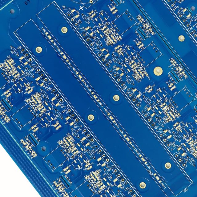
Applications of Heavy Copper PCB
Heavy Copper PCBs are widely used in:
-
Power supply systems
-
Solar inverters
-
Electric vehicle charging systems
-
Industrial motor drives
-
Battery management systems (BMS)
-
Welding equipment
-
Renewable energy systems
These applications demand stable performance under high power conditions.
Heavy Copper PCB vs Standard PCB
| Feature | Standard PCB | Heavy Copper PCB |
|---|---|---|
| Copper Thickness | 1 oz typical | 3 oz+ |
| Current Capacity | Moderate | High |
| Thermal Handling | Limited | Strong |
| Mechanical Strength | Standard | Enhanced |
| Cost | Lower | Higher |
Heavy copper PCB is chosen when performance outweighs cost concerns.
Conclusion
Heavy Copper PCB technology provides robust electrical and thermal performance for high-current and high-power electronic systems. By increasing copper thickness and optimizing layout design, these PCBs enhance reliability, reduce thermal stress, and support demanding industrial and energy applications.
For power electronics and renewable energy systems, Heavy Copper PCB is a dependable and durable solution.
