SiC PCB: Supporting the Next Generation of Power Electronics
With the rapid growth of electric vehicles, renewable energy systems, and industrial power modules, Silicon Carbide (SiC) devices are becoming a key technology in modern power electronics.
Compared to traditional silicon components, SiC devices operate at higher voltages, higher temperatures, and higher switching frequencies. However, these advantages also place much stricter requirements on PCB design and manufacturing.
A well-designed SiC PCB plays a critical role in ensuring electrical stability, thermal efficiency, and long-term reliability.
Why SiC Devices Require Specialized PCB Design
1. High Voltage Capability
SiC MOSFETs and diodes commonly operate at 650V, 1200V, or even higher. PCB layout must ensure:
-
Adequate creepage and clearance distances
-
Optimized insulation structure
-
Controlled electric field distribution
Improper design may lead to partial discharge or breakdown under high voltage stress.
2. High Switching Frequency
SiC devices switch significantly faster than traditional silicon IGBTs. This leads to:
-
Increased EMI risk
-
Higher demand for controlled impedance
-
Reduced parasitic inductance requirements
PCB stack-up design and layout optimization are essential to minimize loop inductance and voltage overshoot.
3. High Temperature Performance
SiC devices can operate at junction temperatures above 175°C. PCB materials must support:
-
High Tg values
-
Low thermal expansion mismatch
-
Stable dielectric properties under heat
Thermal vias, heavy copper layers, and optimized copper balancing help improve heat dissipation.
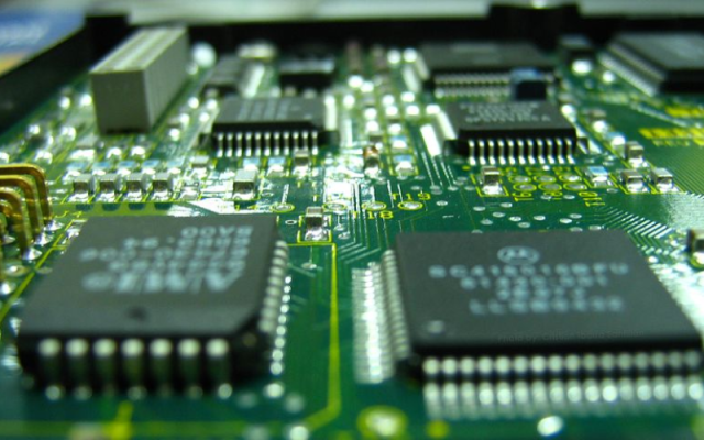
Key Technologies Used in SiC PCB Manufacturing
To support high-power SiC modules, PCB structures often include:
-
Multilayer PCB (4–12+ layers)
-
Heavy copper (2oz–6oz or higher)
-
Thick copper base or IMS (Insulated Metal Substrate)
-
Low-loss and high-Tg materials
-
Controlled impedance routing
-
Press-fit or high-current connector design
For automotive-grade applications, compliance with AEC-related reliability testing is often required.
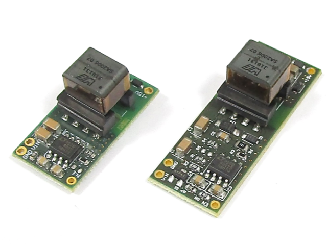
Typical Applications of SiC PCB
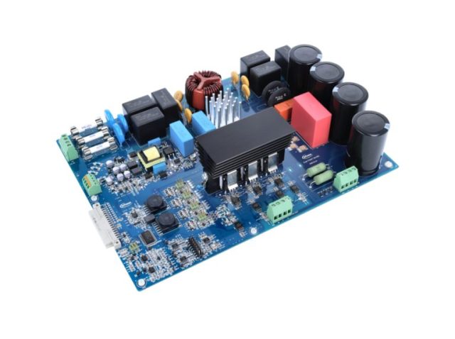
SiC PCBs are widely used in:
-
EV onboard chargers (OBC)
-
DC-DC converters
-
Inverters for electric vehicles
-
Solar inverters
-
Energy storage systems
-
Industrial motor drives
As power density increases, PCB design becomes even more critical in maximizing SiC performance advantages.
Conclusion
SiC technology enables higher efficiency, reduced system size, and improved energy conversion performance. However, without proper PCB design, these benefits cannot be fully realized.
A well-engineered SiC PCB ensures electrical safety, thermal stability, and long-term operational reliability — forming the foundation of next-generation power systems.
