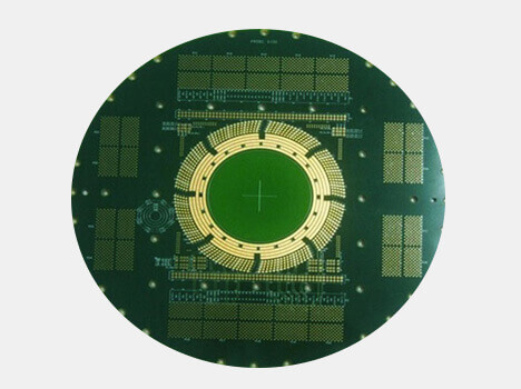
What Is an IoT IC Test PCB?
An IoT IC Test PCB is a specialized printed circuit board used to test Internet of Things (IoT) integrated circuits during development, validation, and mass production. It provides a stable electrical interface between the IoT IC under test (DUT) and automated test equipment (ATE), ensuring accurate functional, RF, and performance testing.
IoT IC test PCBs are widely used for testing MCUs, SoCs, RF transceivers, connectivity chips, and sensor interface ICs used in smart devices and connected systems.
Why IoT IC Testing Needs Dedicated Test PCBs
IoT chips combine low power consumption, wireless communication, and mixed-signal functionality, which makes testing more complex than standard digital ICs. Typical challenges include:
-
Ultra-low power measurement accuracy
-
RF signal stability and isolation
-
Mixed analog and digital signal integrity
-
High pin density in compact packages
-
Repeatable results for mass production
A dedicated IoT IC test PCB ensures consistent, repeatable, and production-ready testing.
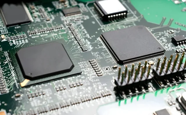
Key Features of IoT IC Test PCBs
High-performance IoT IC test PCBs typically feature:
-
Low-loss signal routing for RF and high-speed interfaces
-
Controlled impedance traces for wireless and communication signals
-
Stable power distribution for low-power measurement
-
Excellent grounding and shielding to reduce noise
-
High mechanical durability for repeated test cycles
These features are essential to ensure accurate testing of both electrical and RF performance.
Design Considerations for IoT IC Test Boards
IoT IC test PCB design requires careful attention to:
-
Separation of RF, analog, and digital domains
-
Optimized impedance matching for antennas and RF ports
-
Short, clean signal paths to minimize interference
-
Solid reference planes for signal return paths
-
Flexible layouts to support various IoT packages
Good design directly impacts test accuracy and yield.
Materials for IoT IC Test PCBs
Material selection depends on signal speed and RF requirements. Common materials include:
-
High-Tg FR-4 for general IoT testing
-
Low-loss laminates for RF and wireless ICs
-
Hybrid stackups for mixed-signal applications
-
Stable dielectric materials for consistent RF performance
These materials help maintain signal integrity across different test conditions.
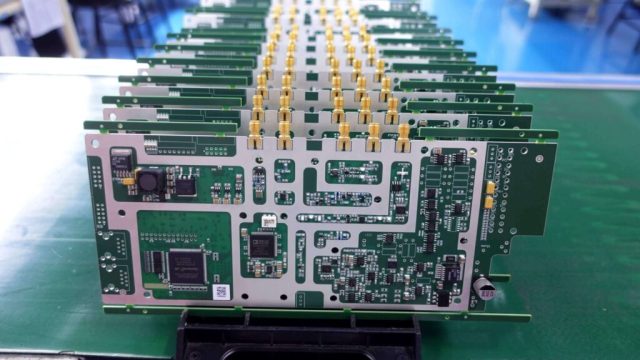
Manufacturing Capabilities for IoT IC Test PCBs
Manufacturing IoT IC test PCBs requires advanced processes such as:
-
Multilayer PCB fabrication
-
Tight impedance control and verification
-
HDI technology for fine-pitch IoT ICs
-
High layer alignment accuracy
-
Automated optical inspection (AOI)
Precision manufacturing ensures reliability in both prototype and volume testing.
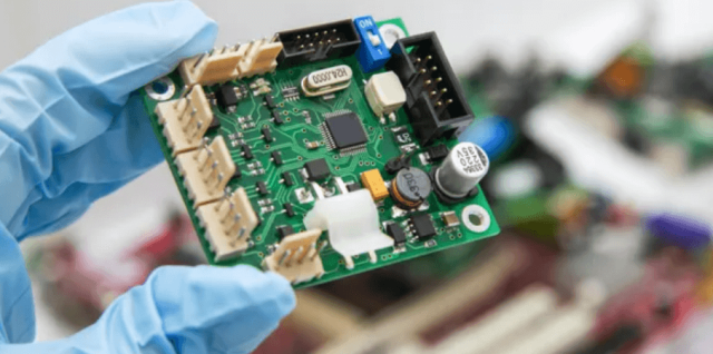
Assembly and Test Interface Integration
IoT IC test PCB assembly may include:
-
IC test sockets and probe interfaces
-
High pin count connectors
-
Precision passive components
-
Stable solder joints for long-term testing
Assembly quality directly affects contact reliability and test repeatability.
Applications of IoT IC Test PCBs
IoT IC test PCBs are widely used in testing chips for:
-
Smart home and smart city devices
-
Wearable electronics
-
Industrial IoT (IIoT) systems
-
Wireless sensor networks
-
Asset tracking and smart metering
-
Medical and healthcare IoT devices
They support testing from early R&D to high-volume production.
Why Choose a Professional IoT IC Test PCB Manufacturer
A reliable IoT IC test PCB supplier offers:
-
Experience in RF and low-power PCB design
-
Stable quality for repeated ATE testing
-
Fast turnaround for prototypes and small batches
-
Support for custom test requirements
-
Engineering assistance from design to assembly
Choosing the right partner helps improve test efficiency and product yield.
