What Is a Package Test PCB?
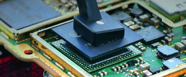
A Package Test PCB is a specialized printed circuit board designed for package-level semiconductor testing, where integrated circuits are tested after packaging but before final shipment. It serves as the electrical and mechanical interface between the packaged IC (DUT) and automated test equipment (ATE).
Package test PCBs are commonly used in final test, system-level test, and reliability testing, ensuring that packaged devices meet electrical and performance specifications before entering the market.
Role of Package Test PCB in Semiconductor Testing
After wafer probing, ICs are assembled into packages such as BGA, LGA, QFN, QFP, or custom packages. A package test PCB enables:
-
Functional and parametric testing of packaged ICs
-
High-speed and high-frequency signal validation
-
Power integrity and thermal performance evaluation
-
Long-duration reliability and stress testing
The quality of the package test PCB directly affects test accuracy, yield, and throughput.
Key Requirements for Package Test PCBs
Compared with standard PCBs, package test PCBs must meet stricter requirements:
-
High pin count support for advanced IC packages
-
Fine pitch routing for BGA and LGA packages
-
Controlled impedance routing for high-speed interfaces
-
Low crosstalk and low skew design
-
Excellent flatness and mechanical stability
-
Durability for repeated socket insertion cycles
These requirements make package test PCBs a critical element in semiconductor production testing.
Design Considerations
Effective package test PCB design typically includes:
-
Optimized multilayer stackup with dedicated power and ground planes
-
Short, matched signal paths to maintain timing accuracy
-
Robust power delivery networks for stable operation
-
Careful socket footprint and keep-out design
-
Reinforcement around socket and connector areas
Close collaboration between PCB designers, socket vendors, and test engineers is essential.
Materials Used in Package Test PCBs
Material selection depends on signal speed and test environment:
-
High-TG FR-4 for standard package-level testing
-
Low Dk / Low Df laminates for high-speed or RF package testing
-
Hybrid stackups for mixed-signal package test PCBs
Stable dielectric properties ensure consistent impedance and repeatable measurements.
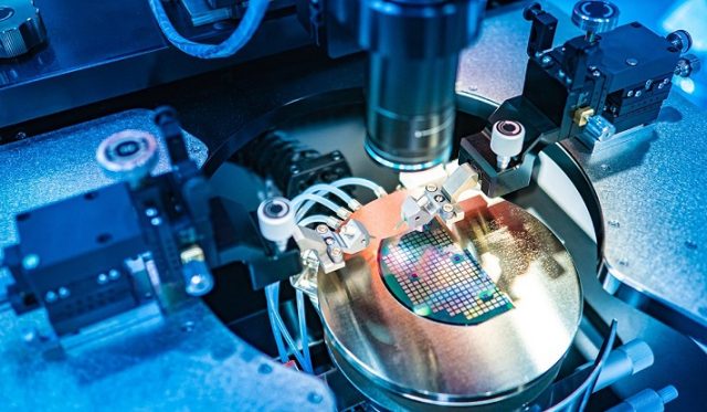
Manufacturing Capabilities for Package Test PCBs
A professional package test PCB manufacturer should support:
-
Multilayer PCB fabrication (commonly 8–24+ layers)
-
HDI PCB technology for fine pitch fan-out
-
Controlled impedance manufacturing and validation
-
Tight tolerance drilling and registration
-
High-reliability surface finishes such as ENIG or ENEPIG
Precision manufacturing ensures consistent performance across production lots.
Assembly Considerations
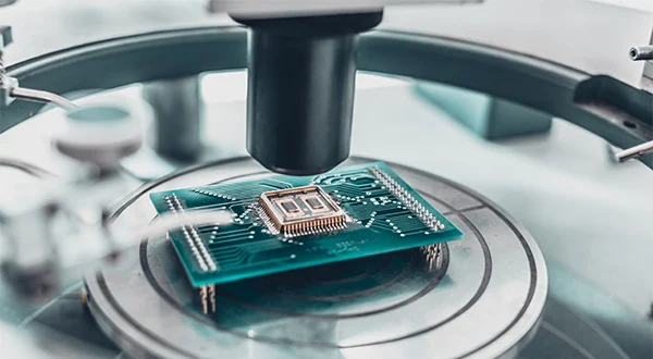
Package test PCB assembly often includes:
-
Mounting of IC test sockets
-
High-speed connectors and interface components
-
Passive components for signal conditioning
-
Mechanical stiffeners or reinforcement if required
Accurate assembly is essential for maintaining electrical integrity and mechanical reliability throughout test cycles.
Applications of Package Test PCBs
Package test PCBs are widely used in:
-
Final test load boards
-
System-level test PCB
-
Logic IC, processor, and SoC testing
-
Memory package testing (DRAM, NAND)
-
RF and mixed-signal IC package testing
They are an indispensable part of high-volume semiconductor manufacturing.
Why Choose a Specialized Package Test PCB Supplier
An experienced package test PCB supplier provides:
-
Deep understanding of package-level testing requirements
-
Optimized stackup and impedance control
-
High yield and long service life
-
Fast prototype and small batch support
-
Engineering assistance from design review to final assembly
Choosing the right supplier helps improve test accuracy, reduce downtime, and increase overall production efficiency.
