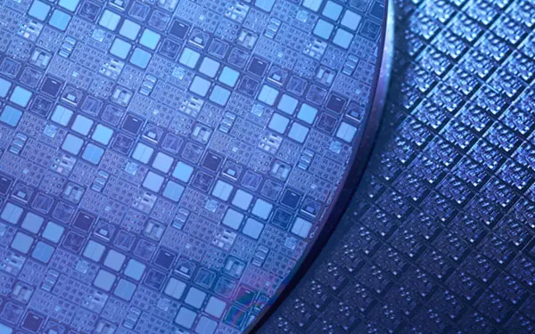
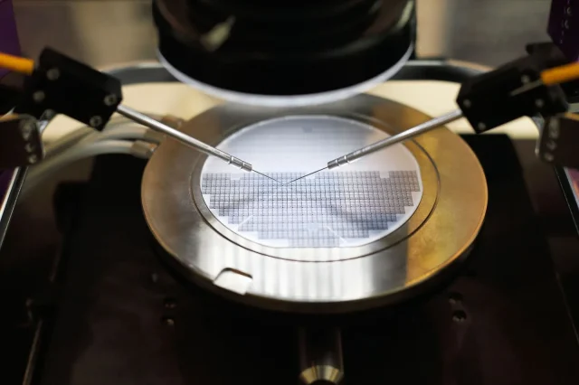
In semiconductor manufacturing, wafer testing is a critical step performed before packaging to verify die functionality and performance. A high-quality Wafer Test PCB serves as the electrical interface between the wafer probe card and automated test equipment (ATE), enabling precise signal transmission and accurate measurement results.
As IC designs continue to scale in speed, density, and complexity, wafer test PCBs must deliver excellent signal integrity, mechanical stability, and repeatable performance under demanding test conditions.
What Is a Wafer Test PCB?
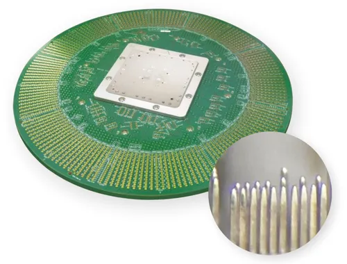
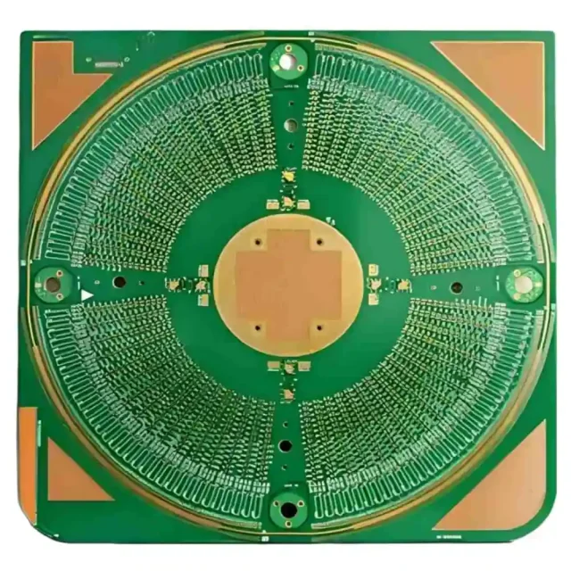
A Wafer Test PCB is a specialized printed circuit board used in wafer-level testing to route signals between the probe card and the ATE system. It supports thousands of probe contacts and high-speed signal paths required for modern semiconductor devices.
Unlike production PCBs, wafer test PCBs are optimized for test accuracy, electrical consistency, and durability rather than long-term field operation.
Key Requirements for Wafer Test PCBs
High Pin Count and Dense Routing
Advanced wafer testing involves a large number of I/O channels. Wafer test PCBs must support fine line routing, dense fan-out, and high pin count connectors.
Controlled Impedance and Signal Integrity
High-speed wafer testing requires strict impedance control, low insertion loss, and minimal crosstalk to ensure accurate test results.
Electrical Stability and Repeatability
Consistent dielectric properties and stable stack-up design are essential to maintain repeatable electrical performance across test cycles.
Mechanical Reliability
Wafer test PCBs experience repeated probe contact, thermal cycling, and long test durations, requiring robust mechanical design and fabrication quality.
Wafer Test PCB Design Considerations
Effective wafer test PCB design typically includes:
-
Multilayer stack-up optimization
-
Controlled impedance routing for high-speed signals
-
Short and matched signal paths
-
Solid power and ground planes
-
Careful connector and probe interface layout
Early collaboration between PCB designers and test engineers helps minimize signal distortion and test variation.
Materials for Wafer Test PCBs
Material selection directly impacts wafer test accuracy. Common materials include:
-
High-Tg FR-4 for general wafer testing
-
Low-loss laminates for high-speed or RF wafer test PCBs
-
Hybrid stack-ups for mixed-signal and high-frequency applications
Stable dielectric constant and low dissipation factor improve measurement consistency.
Manufacturing Capabilities for Wafer Test PCBs
Professional wafer test PCB manufacturing requires:
-
Fine line and spacing capability
-
Multilayer and HDI fabrication
-
Blind and buried via technology when needed
-
Tight thickness and impedance tolerances
-
100% electrical testing and inspection
Precision manufacturing ensures consistent performance from board to board.
Wafer Test PCB Assembly
Many wafer test applications require PCB assembly services, including:
-
High pin count connectors
-
Probe card interface components
-
Fine-pitch SMT assembly
-
Mixed SMT and through-hole technology
Careful assembly reduces mechanical stress and ensures stable electrical connections during testing.
Applications of Wafer Test PCBs
Wafer test PCBs are widely used in:
-
Wafer probe testing
-
Semiconductor R&D validation
-
ATE wafer test systems
-
Process monitoring and yield analysis
Each application demands high accuracy and repeatability.
Prototype and Small Batch Wafer Test PCBs
Semiconductor development often requires prototype or small batch wafer test PCBs for early-stage validation and test program development. Fast turnaround and engineering support are critical to meet tight development schedules.
Small batch wafer test PCBs allow rapid iteration before scaling to full production.
Why Choose a Specialized Wafer Test PCB Manufacturer?
An experienced wafer test PCB manufacturer provides:
-
Deep understanding of wafer-level testing requirements
-
Precision fabrication and strict quality control
-
Support for custom and complex designs
-
Flexible volume from prototype to production
This ensures wafer test PCBs meet the demanding standards of semiconductor testing.
Conclusion
Wafer Test PCB manufacturing is essential for accurate and reliable semiconductor wafer testing. With optimized design, controlled impedance, and high-quality fabrication, wafer test PCBs enable precise measurement, improved yield, and efficient test workflows.
Partnering with a professional wafer test PCB supplier helps ensure consistent test performance and accelerated semiconductor development.
