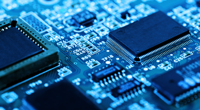
A Semiconductor Testing PCB is a critical interface board used in automated test equipment (ATE) to validate the functionality, performance, and reliability of semiconductor devices. From wafer sort to final test, semiconductor testing PCBs play a key role in ensuring that ICs meet electrical, thermal, and functional specifications before entering the market.
As semiconductor technology advances toward higher speeds, smaller geometries, and higher pin counts, the requirements for semiconductor testing PCBs continue to grow in complexity.
What Is a Semiconductor Testing PCB?
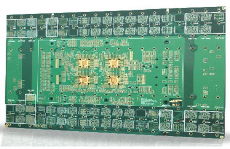
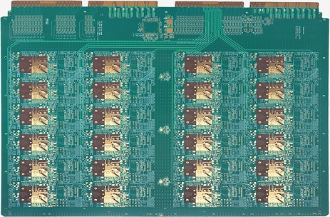
A Semiconductor Testing PCB is specifically designed to connect test instruments to devices under test (DUTs), such as ICs, processors, memory chips, and RF components. These PCBs are commonly used as load boards, interface boards, probe card PCBs, or custom test fixtures within ATE systems.
Unlike standard PCBs, semiconductor testing PCBs prioritize signal integrity, impedance control, and mechanical stability under repeated test cycles.
Key Requirements of Semiconductor Testing PCBs
High Pin Count Support
Modern semiconductor devices often require hundreds or thousands of test points. Semiconductor testing PCBs are designed to handle dense routing and complex pin mappings.
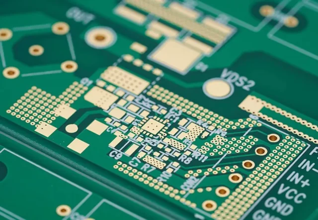
Controlled Impedance
Accurate impedance control is essential for high-speed digital and RF test signals, ensuring repeatable and reliable test results.
High-Speed Signal Integrity
Differential pairs, length matching, and low-loss routing are critical to prevent signal distortion during high-frequency testing.
Power Integrity and Noise Control
Dedicated power and ground layers help maintain stable voltage levels and minimize noise during test operations.
Design Challenges in Semiconductor Testing PCBs
Designing a semiconductor testing PCB involves overcoming multiple technical challenges:
-
Routing ultra-fine pitch components
-
Managing crosstalk in dense multilayer structures
-
Maintaining tight impedance tolerance
-
Ensuring thermal stability during long test cycles
-
Supporting frequent insertion and removal of DUTs
These challenges require deep experience in both PCB design and semiconductor testing environments.
Materials Used in Semiconductor Testing PCBs
Material selection depends on test frequency, operating conditions, and reliability requirements. Common materials include:
-
High-Tg FR-4 for general testing
-
Low-loss laminates for high-speed and RF applications
-
Mixed dielectric stack-ups for hybrid digital/RF testing
-
Advanced prepregs for controlled thickness and impedance
Choosing the right materials is essential for consistent test performance.
Manufacturing Capabilities for Semiconductor Testing PCBs
Producing semiconductor testing PCBs requires advanced fabrication technologies, such as:
-
Multilayer PCB manufacturing (up to 40+ layers)
-
HDI processes with blind and buried vias
-
Laser drilling for fine pitch routing
-
Precise layer registration and lamination control
-
Impedance testing and electrical verification
These capabilities ensure stable electrical characteristics across all boards.
Semiconductor Testing PCB Assembly
Assembly for semiconductor testing PCBs often includes:
-
High pin count socket installation
-
Fine-pitch SMT and through-hole assembly
-
X-ray inspection for hidden solder joints
-
Functional and continuity testing
Assembly quality directly affects test accuracy and board lifespan.
Applications of Semiconductor Testing PCBs
Semiconductor testing PCBs are widely used in:
-
Wafer sort and probe testing
-
Final IC testing and validation
-
Burn-in and reliability testing
-
High-speed logic and memory testing
-
RF and mixed-signal semiconductor testing
These applications demand extreme reliability and precision.
Prototype and Small Batch Semiconductor Testing PCBs
Most semiconductor testing projects begin with prototype or small batch PCBs to verify electrical performance and mechanical compatibility. Rapid prototyping allows engineers to optimize signal integrity and impedance before scaling to production.
A reliable semiconductor testing PCB supplier supports both prototype and volume manufacturing with consistent quality.
Conclusion
A Semiconductor Testing PCB is a foundational component of modern ATE systems, enabling accurate, repeatable, and high-speed semiconductor validation. With high pin count support, controlled impedance, and advanced multilayer designs, these PCBs meet the demanding requirements of today’s semiconductor industry.
Selecting an experienced semiconductor testing PCB manufacturer is essential to ensure performance, reliability, and long-term success.
