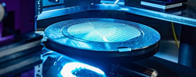
A Custom Probe Card PCB is a highly specialized printed circuit board designed for semiconductor wafer testing in automated test equipment (ATE) systems. As semiconductor devices continue to move toward advanced process nodes, higher pin counts, and higher signal speeds, probe card PCBs must meet extremely demanding requirements for precision, signal integrity, and mechanical reliability.
Custom probe card PCB manufacturing plays a critical role in ensuring accurate electrical contact, stable signal transmission, and repeatable test performance throughout high-volume wafer testing.
What Is a Custom Probe Card PCB?
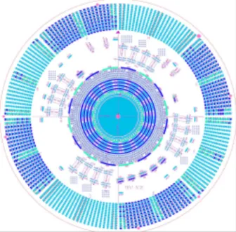
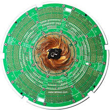
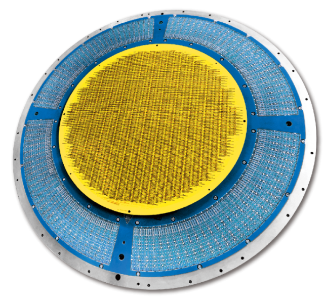
A Custom Probe Card PCB is the core structural and electrical platform of a probe card assembly. It provides the interconnection between probe needles or MEMS probe elements and the ATE system, enabling electrical testing of semiconductor wafers before packaging.
Unlike standard PCBs, custom probe card PCBs are engineered specifically for wafer-level testing and must meet strict tolerances for flatness, impedance, layer alignment, and via reliability.
Key Requirements for Custom Probe Card PCB Manufacturing
Ultra-High Precision and Flatness
Custom probe card PCBs require excellent dimensional accuracy and planarity to ensure uniform probe contact across the entire wafer surface.
High Pin Count and Dense Interconnection
Modern ICs demand custom probe card PCBs capable of supporting hundreds or thousands of signal channels within limited PCB area.
Controlled Impedance and Signal Integrity
High-speed digital and RF wafer testing requires precise impedance control to minimize signal reflection, skew, and measurement error.
Mechanical and Thermal Reliability
Probe card PCBs must withstand repeated probing cycles, vibration, and thermal variation without performance degradation.
Materials Used in Custom Probe Card PCB Manufacturing
Material selection directly impacts the performance and durability of a custom probe card PCB.
Common material options include:
-
High-Tg FR-4 for standard wafer probe applications
-
Low-loss laminates for high-speed and RF probe card PCBs
-
Hybrid stack-ups combining FR-4 and low-Df materials
-
Specialized materials for enhanced thermal and mechanical stability
An experienced custom probe card PCB manufacturer assists in selecting materials based on electrical performance and test environment requirements.
Manufacturing Capabilities for Custom Probe Card PCBs
Producing reliable custom probe card PCBs requires advanced PCB fabrication technology and strict process control:
-
Multilayer and high layer count PCB fabrication
-
Fine line and space etching for dense signal routing
-
Controlled impedance PCB manufacturing
-
Robust via plating for long probe card life
-
Precision lamination and thickness control
-
Electrical testing and impedance verification
These capabilities ensure consistent electrical and mechanical performance in wafer test environments.
Design Challenges and Engineering Support
Custom probe card PCB design involves multiple technical challenges:
-
Dense fan-out routing from wafer contacts
-
Crosstalk and noise control for high-speed signals
-
Power and ground plane optimization
-
Integration with probe needles and MEMS structures
-
Reliability under high-cycle mechanical stress
Professional manufacturers provide DFM review, signal integrity analysis, and close engineering collaboration to improve first-pass success.
Applications of Custom Probe Card PCBs
Custom probe card PCBs are widely used in:
-
Semiconductor wafer probe and wafer sort testing
-
Logic, memory, and mixed-signal IC testing
-
RF and mmWave wafer-level testing
-
Advanced-node semiconductor validation
-
High-volume manufacturing test systems
In all these applications, the quality of the custom probe card PCB directly affects test accuracy, yield, and throughput.
From Prototype to Volume Production
Custom probe card PCB projects typically start with prototype fabrication to validate electrical performance, flatness, and mechanical durability. After qualification, the same materials and processes are used for small-batch or volume production to ensure consistent performance across multiple probe card assemblies.
Working with a single supplier from prototype through production ensures long-term stability and supply continuity.
Conclusion
A Custom Probe Card PCB is a mission-critical component in semiconductor wafer testing and ATE systems. Through high-precision manufacturing, controlled impedance design, and advanced multilayer technology, professional PCB suppliers deliver custom probe card PCBs that support accurate, repeatable, and reliable wafer-level testing.
As semiconductor technologies continue to advance, partnering with an experienced custom probe card PCB manufacturer is essential for meeting the demands of next-generation wafer test applications.
