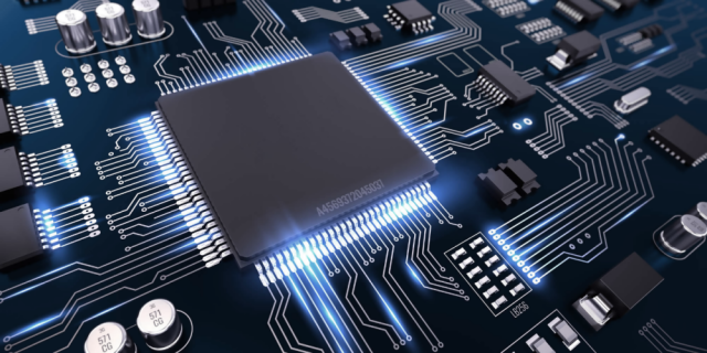
A Multilayer Test PCB is a critical component used in electronic and semiconductor testing environments, including automated test equipment (ATE), functional testing systems, and reliability validation platforms. As test requirements become more complex and signal speeds increase, multilayer test PCBs are essential for supporting dense routing, stable signal transmission, and long-term mechanical reliability.
Professional multilayer test PCB manufacturing ensures accurate test results, repeatable performance, and extended service life in high-cycle test conditions.
What Is a Multilayer Test PCB?
A Multilayer Test PCB is a printed circuit board consisting of multiple conductive layers designed specifically for test and validation purposes. These PCBs act as the interface between the device under test (DUT) and the test system, enabling signal routing, power distribution, and measurement access.
Compared to standard PCBs, multilayer test PCBs require higher durability, tighter impedance control, and more robust mechanical design.
Key Requirements of Multilayer Test PCBs
High Signal Integrity
Multilayer test PCBs often handle high-speed digital, analog, and RF signals. Precise controlled impedance and optimized stack-up design are essential to minimize signal loss, reflection, and crosstalk.
Mechanical Strength and Durability
Test PCBs experience repeated insertion, probing, and mechanical stress. Strong via structures, thick copper plating, and reinforced materials ensure long service life.
Thermal Stability
Power-intensive test operations generate heat. Multilayer test PCBs must maintain stable electrical performance across temperature variations.
Manufacturing Consistency
Consistent PCB quality is critical to ensure reliable and repeatable test results across multiple test systems and production batches.
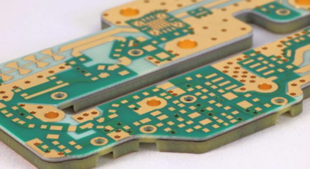
Materials Used in Multilayer Test PCB Manufacturing
Material selection depends on signal speed, test conditions, and durability requirements:
-
High-Tg FR-4 for standard test applications
-
Low-loss materials for high-speed or RF test PCBs
-
Hybrid stack-ups combining FR-4 with high-frequency laminates
-
Thick copper constructions for power and stress testing
An experienced multilayer test PCB manufacturer assists in selecting the optimal material combination.
Manufacturing Capabilities for Multilayer Test PCBs
Producing reliable multilayer test PCBs requires advanced fabrication processes:
-
Multilayer lamination and high layer count capability
-
Controlled impedance PCB processing
-
Fine line and space etching
-
Robust via plating for long-term durability
-
Hard gold or ENIG surface finishes for test interfaces
-
Electrical testing and impedance verification
These capabilities ensure long-term performance in demanding test environments.
Design Challenges and Engineering Support
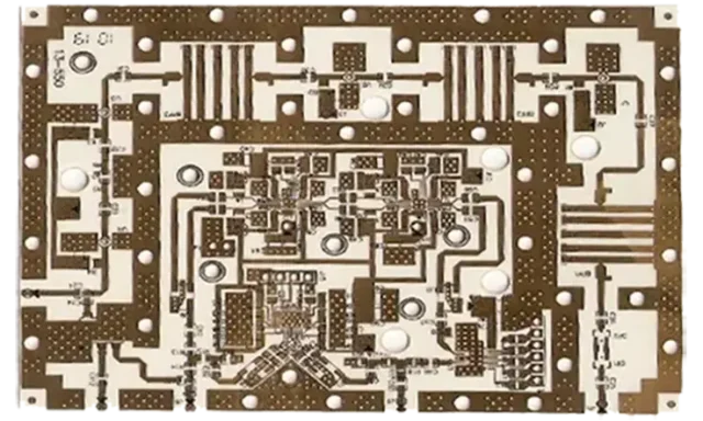
Designing a multilayer test PCB presents several challenges:
-
High-density routing for large pin-count devices
-
Signal isolation and noise control
-
Power and ground plane optimization
-
Connector, socket, and probe interface integration
-
EMI and grounding strategies
Professional test PCB suppliers provide DFM and engineering support to improve manufacturability and test reliability.
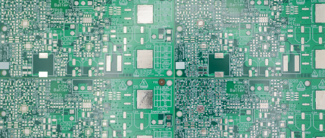
Applications of Multilayer Test PCBs
Multilayer test PCBs are widely used in:
-
Automated test equipment (ATE)
-
Semiconductor wafer and package testing
-
Load boards and test interface boards
-
Logic and functional test systems
-
Burn-in and reliability testing
-
Automotive and industrial electronics testing
In these applications, PCB reliability directly affects test accuracy and uptime.
From Prototype to Volume Production
Multilayer test PCB projects often begin with prototype builds to validate signal performance, mechanical durability, and connector reliability. Once confirmed, the same materials and manufacturing processes are scaled to small-batch or volume production, ensuring consistency across all test systems.
Conclusion
A Multilayer Test PCB is a mission-critical component for modern electronic testing systems. By combining precise impedance control, robust mechanical design, and advanced manufacturing processes, professional multilayer test PCB manufacturers deliver reliable solutions for high-speed and high-cycle test environments.
As testing requirements continue to grow in complexity, choosing an experienced multilayer test PCB supplier is essential for achieving accurate, repeatable, and scalable test performance.
