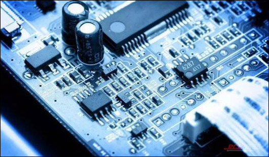
A controlled impedance PCB prototype is a critical step in validating high-speed and high-frequency electronic designs before mass production. As data rates increase and signal frequencies rise, maintaining precise impedance values becomes essential to ensure signal integrity, reduce reflection, and minimize transmission loss.
Controlled impedance PCB prototypes are widely used in applications such as high-speed digital systems, RF communication, 5G modules, automotive electronics, and semiconductor test equipment.
What Is a Controlled Impedance PCB Prototype?
A controlled impedance PCB prototype is a prototype PCB manufactured with tightly controlled trace impedance values, such as 50Ω single-ended or 90Ω/100Ω differential impedance. Unlike standard PCBs, impedance-controlled prototypes require precise coordination between design, materials, stack-up, and fabrication processes.
These prototypes allow engineers to verify electrical performance, timing, and signal quality before scaling to mass production.
Why Controlled Impedance Is Critical in PCB Prototyping
High-speed and high-frequency signals are extremely sensitive to impedance variations. Without proper impedance control, signal reflections, crosstalk, and eye diagram degradation can occur.
A controlled impedance PCB prototype helps to:
-
Validate signal integrity at the prototype stage
-
Reduce design risk before production
-
Ensure compliance with high-speed interface standards
-
Improve overall system reliability
-
Shorten development cycles
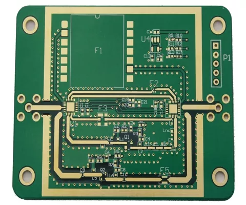
Typical Impedance Types in PCB Prototypes
Controlled impedance PCB prototypes commonly support:
-
Single-ended impedance (e.g. 50Ω, 75Ω)
-
Differential impedance (e.g. 90Ω, 100Ω, 110Ω)
-
Microstrip and stripline structures
-
High-speed serial interfaces (USB, HDMI, PCIe, Ethernet)
-
RF and microwave transmission lines
Each impedance type requires accurate calculation and manufacturing control.
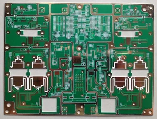
Stack-Up and Material Selection
The stack-up design is the foundation of a reliable controlled impedance PCB prototype.
PCB Stack-Up Design
Key parameters include:
-
Dielectric thickness
-
Copper weight
-
Trace width and spacing
-
Reference plane structure
Precise stack-up planning ensures impedance consistency across the entire PCB.
Material Selection
Depending on frequency and performance requirements, common materials include:
-
High Tg FR-4 for standard high-speed designs
-
Low-loss laminates for RF and microwave prototypes
-
Rogers and Taconic materials for high-frequency applications
Material stability directly affects impedance accuracy and repeatability.
Manufacturing Process for Controlled Impedance PCB Prototype
Producing a controlled impedance PCB prototype requires advanced fabrication capabilities:
-
Precision etching and trace width control
-
Tight dielectric thickness tolerance
-
Advanced lamination processes
-
Impedance simulation and verification
-
TDR (Time Domain Reflectometry) testing
Professional manufacturers provide impedance reports to confirm that the prototype meets design specifications.
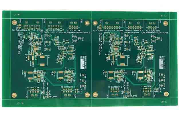
Applications of Controlled Impedance PCB Prototypes
Controlled impedance PCB prototypes are widely used in:
-
High-speed digital systems
-
RF and wireless communication modules
-
5G base stations and IoT devices
-
Automotive ADAS and infotainment systems
-
Semiconductor test and ATE systems
-
Data center and networking equipment
In all these applications, impedance accuracy is essential for functional validation.
From Prototype to Production
A major advantage of working with an experienced manufacturer is the seamless transition from controlled impedance PCB prototype to mass production. Consistent materials, stack-up, and process control ensure performance stability and scalability.
Early impedance verification at the prototype stage significantly reduces redesign costs and delays during production.
Conclusion
A controlled impedance PCB prototype is essential for verifying signal integrity in high-speed and high-frequency electronic designs. By combining precise stack-up design, suitable materials, and advanced manufacturing processes, impedance-controlled prototypes help engineers validate performance, reduce risk, and accelerate product development.
Choosing a professional PCB prototype manufacturer ensures reliable impedance control, accurate testing, and smooth transition from prototype to full-scale production.
