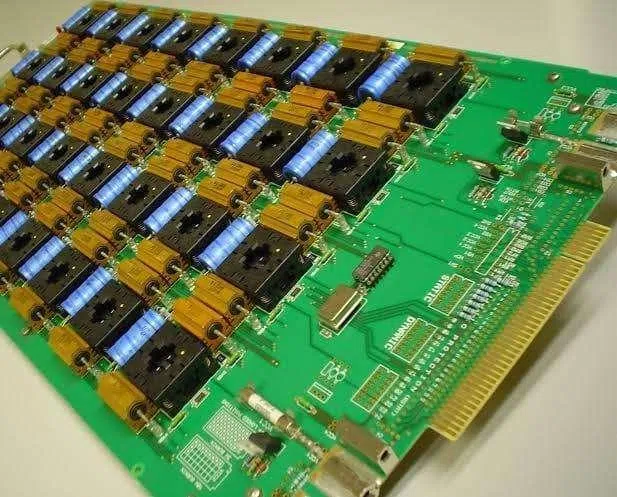
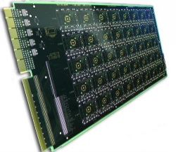
A Burn-in PCB is a specialized test interface designed for accelerated semiconductor reliability screening under sustained electrical and thermal stress. In burn-in systems, the PCB is exposed to continuous high temperature, elevated voltage, and long operating cycles, making it one of the most mechanically and electrically stressed PCB types in semiconductor test environments.
Unlike functional test or characterization boards, a burn-in PCB must prioritize long-term stability and failure resistance over short-term performance optimization.
Engineering Purpose of Burn-in PCBs
The primary objective of burn-in testing is to identify early-life device failures by forcing latent defects to manifest under extreme operating conditions. The burn-in PCB provides:
-
Electrical connectivity between the DUT and the burn-in system
-
Power delivery paths capable of continuous high current
-
Signal routing for monitoring device response during stress
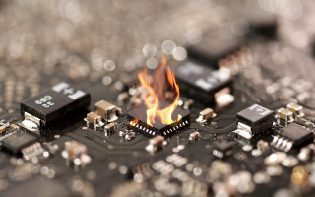
Any PCB-related drift or failure can mask device defects or introduce false failures, directly compromising test validity.
Thermal Stress and Material Selection
Burn-in PCBs typically operate at temperatures ranging from 125°C to 175°C, and in some advanced applications even higher. This makes material selection a fundamental design decision.
Key material requirements include:
-
High TG laminates to prevent resin softening and delamination
-
Stable dielectric properties at elevated temperature
-
Low Z-axis expansion to protect plated through holes
-
Strong adhesion between copper and dielectric layers
Standard FR-4 materials often struggle under long-duration burn-in conditions, leading to via fatigue, pad lifting, or dielectric degradation.
Power Integrity Under Continuous Load
Unlike short-duration test boards, burn-in PCBs must handle sustained power delivery without degradation. Design considerations include:
-
Wide power planes and low-resistance copper paths
-
Optimized via arrays for current sharing
-
Controlled temperature rise across copper structures
-
Balanced copper distribution to reduce thermal gradients
Poor power integrity design can result in localized overheating, accelerating PCB aging and reducing burn-in fixture lifetime.
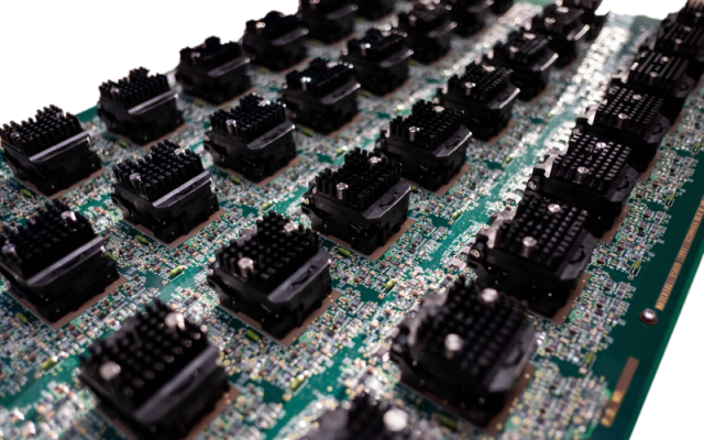
Mechanical Reliability and Repetitive Stress
Burn-in PCBs are repeatedly subjected to:
-
Socket insertion and removal
-
Thermal expansion and contraction cycles
-
Long-term mechanical loading inside ovens or chambers
To address these challenges, burn-in PCB design emphasizes:
-
Controlled CTE matching between materials
-
Robust pad and via structures
-
Reinforced connector regions
-
Warpage control through symmetric stackups
Mechanical failures often occur gradually, making upfront structural margin essential.
Manufacturing Consistency and Process Control
From a manufacturing standpoint, burn-in PCBs demand exceptional process stability. Key production controls include:
-
Tight lamination pressure and temperature profiles
-
Accurate drilling and via plating for high aspect ratio holes
-
Uniform copper thickness across layers
-
100% electrical testing and thermal process validation
Because burn-in boards are often used across multiple test cycles and long timeframes, consistency between builds is critical.
Typical Burn-in PCB Applications
Burn-in PCBs are widely used in:
-
Semiconductor reliability screening systems
-
Automotive-grade IC qualification
-
Power device burn-in (MOSFET, IGBT, SiC, GaN)
-
High-temperature logic and memory device testing
-
Long-duration stress test platforms
These applications prioritize durability, repeatability, and thermal resilience over aggressive miniaturization.
Engineering Perspective
From an engineering perspective, a burn-in PCB is not a disposable test accessory—it is a reliability-critical subsystem. Its design and fabrication directly influence test accuracy, fixture uptime, and overall screening effectiveness.
KKPCB supports burn-in PCB projects through high-TG material selection, reinforced via structures, power integrity optimization, and tightly controlled manufacturing processes, delivering stable performance in extreme test environments.
