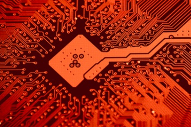
Mixed Signal IC Test PCB: Bridging Analog Precision and Digital Speed
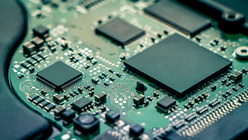
A Mixed Signal IC Test PCB is a specialized printed circuit board designed to test ICs that integrate both analog and digital circuits on a single chip. These devices often combine high-speed digital logic with sensitive analog functions, such as ADCs, DACs, RF front-ends, power management blocks, and sensor interfaces.
To ensure accurate device characterization and production testing, mixed signal IC test PCBs must deliver clean analog signal paths, stable power distribution, controlled impedance routing, and minimal noise coupling between analog and digital domains.
Key Design Challenges in Mixed Signal IC Test PCBs
1. Analog and Digital Signal Isolation
One of the most critical aspects of a mixed signal IC test PCB is proper isolation between analog and digital circuits. Layout strategies such as split ground planes, controlled return paths, and strategic component placement are essential to reduce noise coupling and signal distortion.
2. High-Speed Digital Signal Integrity
Digital test channels often operate at high frequencies or fast edge rates, requiring controlled impedance traces, length matching, and low-jitter routing. Any impedance discontinuity can lead to measurement errors during IC testing.
3. Low-Noise Analog Performance
Analog test circuits demand low-noise routing, short signal paths, and stable reference voltages. A mixed signal IC test PCB must minimize crosstalk, EMI, and ground bounce to preserve signal accuracy.
4. Power Integrity and Decoupling
Multiple voltage domains are common in mixed signal ICs. Proper power plane design, decoupling capacitor placement, and low-inductance vias are essential to maintain stable test conditions.
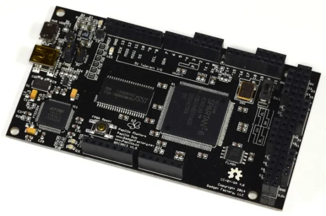
Structural Features of Mixed Signal IC Test PCBs
-
Multilayer PCB stackups to separate analog, digital, and power layers
-
Controlled impedance traces for high-speed digital and clock signals
-
High-density routing to support high pin count ICs and fine-pitch packages
-
Low-loss and low-Dk materials for accurate signal transmission
-
Blind and buried vias or microvias to optimize routing density and reduce parasitics
These features ensure repeatable, high-accuracy IC test results across development, validation, and volume production.
Applications of Mixed Signal IC Test PCBs
Mixed signal IC test PCBs are widely used in:
-
Automated Test Equipment (ATE) systems
-
Semiconductor load boards and test sockets
-
ADC / DAC and data converter testing
-
RF and wireless mixed signal IC testing
-
Automotive electronics and sensor IC validation
-
IoT, industrial control, and power management IC testing
Each application demands high reliability, precise signal control, and stable electrical performance.
Manufacturing Requirements for Mixed Signal IC Test PCBs
Producing high-quality mixed signal IC test PCBs requires:
-
Tight impedance and trace width tolerances
-
Advanced multilayer lamination and registration control
-
Precision drilling and via plating
-
Electrical testing for signal continuity and impedance accuracy
-
Support for prototype, small batch, and production volumes
A reliable PCB manufacturer ensures consistent quality, fast delivery, and repeatable performance for semiconductor testing environments.
Conclusion
A Mixed Signal IC Test PCB plays a critical role in accurate validation of modern integrated circuits that combine analog sensitivity with digital speed. Through careful layout, controlled impedance routing, robust power integrity design, and advanced multilayer construction, these test boards enable precise, repeatable, and reliable IC testing.
Choosing an experienced mixed signal IC test PCB manufacturer ensures high manufacturing quality, stable test performance, and efficient support from prototype to production, helping semiconductor companies reduce test risk and accelerate product qualification.
