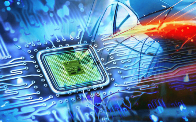
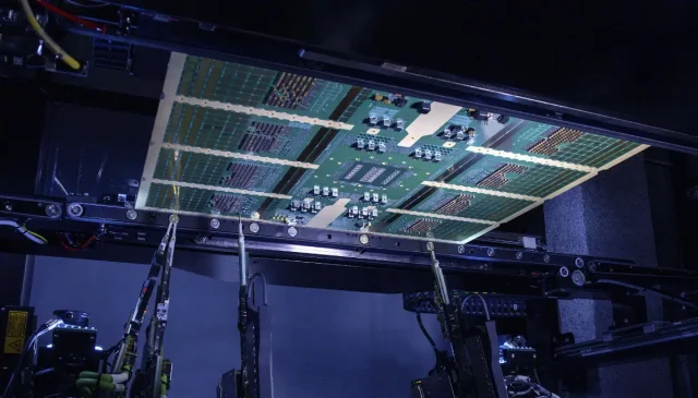
In modern semiconductor testing, probe card assembly PCBs play a vital role in connecting wafer-level devices to automated test equipment (ATE). These specialized PCBs act as the interface between probe cards and the testing system, ensuring high-speed, high-density, and accurate signal transmission for ICs, memory modules, and RF/microwave chips.
High-quality probe card assembly PCBs enable engineers to perform functional, parametric, and wafer-level testing efficiently, ensuring reliable results, minimal errors, and faster time-to-market.
What Is a Probe Card Assembly PCB?
A Probe Card Assembly PCB is a specially designed PCB that integrates with a probe card to facilitate semiconductor wafer testing. Key functions include:
-
Routing high-density signals from wafer pads to ATE systems
-
Providing controlled impedance for high-speed and RF signals
-
Maintaining mechanical stability for accurate probe alignment
-
Supporting high pin count ICs and fine-pitch memory or RF devices
These PCBs are engineered to deliver precision, repeatability, and reliability in demanding semiconductor test environments.
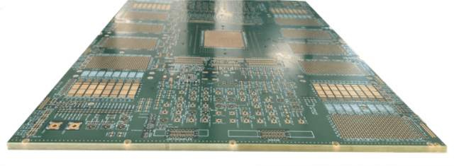
Key Features of Probe Card Assembly PCBs
-
High-Density Signal Routing
Supports complex ICs, memory modules, and RF chips with hundreds or thousands of I/O pins. -
Controlled Impedance
Ensures accurate high-speed signal transmission, minimizing crosstalk and signal reflections. -
Multilayer HDI Design
Separates power, ground, and signal layers to optimize signal integrity for high-frequency applications. -
Mechanical Precision
Maintains probe card alignment, reduces pad damage, and ensures consistent testing over multiple cycles. -
Thermal and Electrical Reliability
Withstands repeated test cycles, burn-in testing, and high-current or high-frequency applications.
Materials and Stackup Considerations
Selecting the proper materials and stackup is crucial for probe card assembly PCB performance:
-
High-Tg FR-4 – Suitable for standard IC and memory module testing
-
Low-Loss Laminates – Required for RF/microwave chip testing
-
Hybrid Stackups – Combine FR-4 and low-loss cores for optimal signal integrity
-
Thermally Stable Materials – Maintain mechanical stability during burn-in or high-current testing
Correct material selection ensures signal integrity, low loss, and reliable probe alignment.
Applications of Probe Card Assembly PCBs
Probe card assembly PCBs are widely used in:
-
Wafer-level IC testing using ATE systems
-
Memory module validation (DRAM, SRAM, Flash)
-
RF and microwave chip functional and parametric testing
-
High-speed and high-frequency semiconductor validation
-
Prototype and small-batch testing before full-scale production
These applications require high-density routing, controlled impedance, mechanical precision, and repeatable performance, all delivered by expertly designed probe card assembly PCBs.
Choosing a Probe Card Assembly PCB Manufacturer
When selecting a manufacturer, key factors include:
-
Experience in high-density, multilayer, and high-pin-count PCB fabrication
-
Expertise with controlled impedance and low-loss materials for high-speed or RF applications
-
Support for prototype, small-batch, and volume production
-
Strong quality control and electrical verification processes
-
Engineering support for design iteration and test system integration
A professional partner ensures accurate, repeatable, and reliable probe card testing for all semiconductor applications.
Conclusion
Probe Card Assembly PCBs are essential for semiconductor wafer-level testing, providing high-density routing, controlled impedance, mechanical stability, and thermal reliability. Partnering with an experienced manufacturer ensures accurate IC, memory, and RF/microwave testing, faster design validation, and a smooth transition from prototype to full-scale production.
