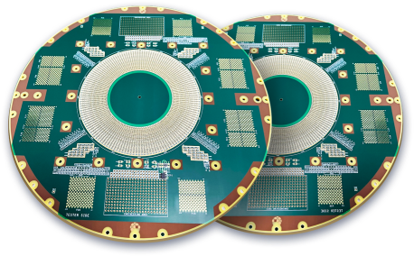
In advanced semiconductor manufacturing, wafer-level testing demands extreme precision and consistency. Probe Card PCB Assembly is a critical process that directly affects test accuracy, yield stability, and long-term reliability. Unlike conventional PCB assembly, probe card PCB assembly requires ultra-tight tolerances, stable mechanical structures, and controlled electrical performance.
A professionally executed probe card PCB assembly ensures accurate signal transmission between automated test equipment (ATE) and the device under test (DUT).
What Makes Probe Card PCB Assembly Unique?
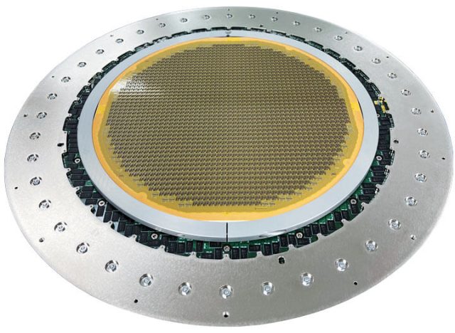
Probe Card PCB Assembly involves assembling high-density, high-layer-count PCBs that interface directly with probe needles or MEMS probes. These PCBs must support:
-
Ultra-high pin count interconnections
-
Fine-pitch probe interfaces
-
High-speed and mixed-signal testing
Every probe card PCB assembly is customized to match specific wafer layouts and test requirements.
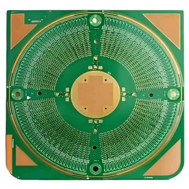
Precision Requirements in Probe Card PCB Assembly
Precision is the defining characteristic of probe card PCB assembly. Key requirements include:
-
Accurate component placement for high-speed connectors
-
Strict control of coplanarity and flatness
-
Stable alignment between PCB, stiffener, and probe structure
Even minor deviations can impact probing accuracy and repeatability.
Signal Integrity in Probe Card PCB Assembly
Modern wafer-level testing operates at increasingly higher frequencies. Probe card PCB assembly must preserve signal integrity by:
-
Minimizing parasitic inductance and capacitance
-
Maintaining controlled impedance throughout assembled interfaces
-
Reducing signal discontinuities at solder joints and connectors
Proper assembly ensures clean, repeatable measurement results.
Power Integrity and Noise Control
Reliable probe card PCB assembly also focuses on power delivery and grounding. This includes:
-
Low-impedance power paths
-
Robust ground connections
-
Effective noise isolation between signal domains
Stable power integrity prevents false failures during testing.
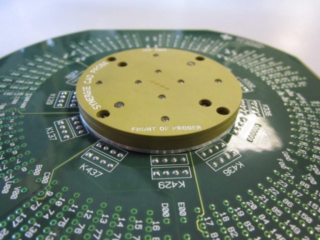
Mechanical Stability and Long-Term Reliability
Probe cards experience repeated contact cycles and thermal variation. High-quality probe card PCB assembly ensures:
-
Strong solder joint reliability
-
Resistance to mechanical stress and vibration
-
Long-term dimensional stability
Mechanical reliability is essential for consistent wafer probing.
Quality Control in Probe Card PCB Assembly
Given the critical nature of semiconductor testing, probe card PCB assembly requires advanced inspection, including:
-
Automated optical inspection (AOI)
-
X-ray inspection for hidden solder joints
-
Electrical continuity and impedance verification
Comprehensive quality control minimizes latent defects.
Small Batch and Production Probe Card PCB Assembly
Probe card PCB assembly often supports:
-
Engineering and characterization builds
-
Qualification and reliability testing
-
Repeatable small-batch and production assembly
Consistent assembly processes ensure uniform performance across multiple probe cards.
Applications of Probe Card PCB Assembly
Probe card PCB assemblies are widely used in:
-
Wafer-level IC testing
-
Logic, memory, and RF semiconductor probing
-
Advanced-node device characterization
-
High-speed and mixed-signal test platforms
Each application demands high precision and stability.
Choosing a Probe Card PCB Assembly Manufacturer
When selecting a probe card PCB assembly supplier, key considerations include:
-
Proven experience with semiconductor testing PCBs
-
Capability for fine-pitch, high-density PCB assembly
-
Strong process control and quality systems
-
Engineering support for NPI and yield optimization
An experienced partner ensures reliable and scalable assembly solutions.
Conclusion
Probe Card PCB Assembly is a mission-critical process in wafer-level semiconductor testing. By combining precision assembly, stable signal integrity, and rigorous quality control, professional probe card PCB assembly enables accurate testing, higher yield, and long-term reliability.
Choosing a specialized probe card PCB assembly manufacturer is essential for achieving consistent and repeatable test performance in advanced semiconductor applications.
