In wafer-level semiconductor testing, even microscopic assembly deviations can lead to unstable probe contact and inconsistent measurements. Probe Card PCB Assembly is a highly specialized process that integrates probe structures, connectors, and high-density routing into a mechanically and electrically stable test platform.
A professionally executed probe card PCB assembly directly determines test accuracy, probe lifetime, and overall wafer test yield.
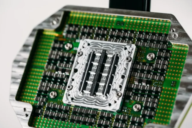
What Is Probe Card PCB Assembly?
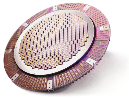
Probe Card PCB Assembly refers to the precision assembly of components and probe interfaces onto a probe card PCB. This includes:
-
Mounting probe needles or MEMS probe structures
-
Assembling high-pin-count connectors
-
Integrating signal conditioning and grounding elements
The assembly process transforms a fabricated PCB into a functional wafer test interface.
Why Assembly Precision Is Critical for Probe Cards
Probe card applications demand:
-
Micron-level alignment accuracy
-
Consistent electrical contact across all probes
-
Mechanical stability under repeated touchdowns
Any assembly inconsistency can result in false test failures or reduced probe life.
Signal Integrity Preservation During Assembly
High-frequency and sensitive signals require careful handling during assembly. Key considerations include:
-
Maintaining controlled impedance at probe interfaces
-
Minimizing parasitic effects introduced by solder joints
-
Preserving short and symmetrical signal paths
Proper assembly ensures clean signal transmission from probe to tester.
Grounding and Noise Control at the Assembly Level
Effective grounding is essential for wafer testing. Probe card PCB assembly incorporates:
-
Low-inductance ground connections
-
Ground shielding around critical signal areas
-
Via stitching and plane continuity
These measures reduce noise and improve measurement repeatability.
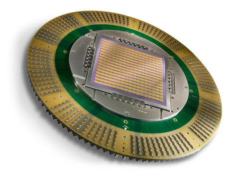
Mechanical Flatness and Coplanarity Control
Probe card PCB assemblies must maintain:
-
Excellent flatness across the board
-
Tight coplanarity between probes
-
Structural integrity under thermal cycling
Mechanical precision ensures uniform probe contact across the wafer.
Material Handling and Thermal Stability
Assembly processes must account for:
-
Material CTE differences
-
Thermal stress during soldering
-
Long-term dimensional stability
Controlled assembly conditions help preserve PCB and probe integrity.
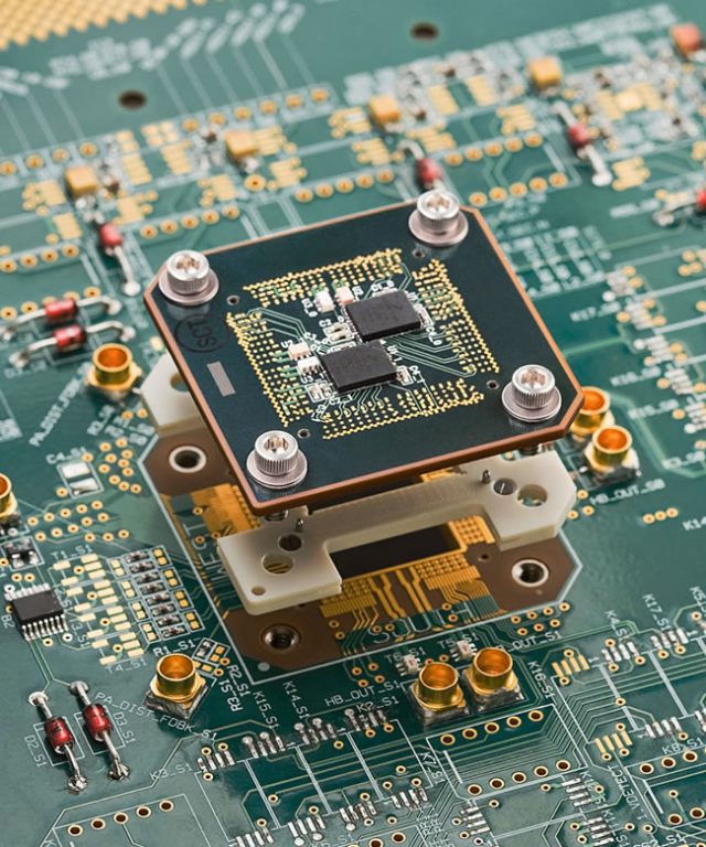
Inspection and Quality Control in Probe Card Assembly
High-quality probe card PCB assembly includes:
-
Optical inspection for alignment and solder quality
-
Electrical continuity and isolation testing
-
Functional verification under test conditions
Strict QC ensures consistent assembly performance.
Applications of Probe Card PCB Assembly
Probe card PCB assemblies are widely used in:
-
Wafer-level parametric testing
-
High-frequency and mixed-signal IC testing
-
Logic, memory, and advanced-node semiconductor testing
-
Engineering validation and volume wafer screening
Each application demands extreme precision and stability.
Selecting a Probe Card PCB Assembly Partner
When choosing a probe card PCB assembly supplier, consider:
-
Experience with wafer-level test hardware
-
Capability for fine-pitch and high-density assembly
-
Controlled impedance and RF assembly expertise
-
Support for prototype and low-volume production
A specialized assembly partner ensures reliable wafer testing performance.
Conclusion
Probe Card PCB Assembly is a mission-critical step in wafer-level semiconductor testing. Through precision alignment, controlled electrical integration, and rigorous quality control, professional probe card PCB assembly enables accurate, repeatable, and high-yield wafer testing.
Partnering with an experienced probe card PCB assembly manufacturer ensures long-term stability and testing confidence in advanced semiconductor applications.
