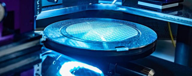
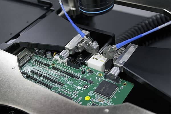
Wafer-level testing is one of the most critical stages in semiconductor manufacturing. At the heart of this process lies the Custom Probe Card PCB, a highly specialized interface board that connects probe needles to automated test equipment with extreme accuracy.
Unlike conventional test boards, custom probe card PCBs must meet strict electrical, mechanical, and dimensional requirements to ensure reliable wafer testing.
What Is a Custom Probe Card PCB?
A Custom Probe Card PCB is a precision-engineered printed circuit board used in semiconductor probe cards to:
-
Route test signals between probes and ATE systems
-
Maintain accurate impedance and signal timing
-
Provide mechanical support for probe structures
Each probe card PCB is uniquely designed for a specific device and test platform.
Why Custom Design Is Essential for Probe Card PCBs
Probe card PCBs operate at the intersection of high-speed signals and micron-level mechanical tolerances. Custom designs allow:
-
Precise alignment of probe contact points
-
Controlled impedance for high-speed testing
-
Adaptation to different wafer sizes and pad layouts
Standard PCBs cannot meet these requirements.
Signal Integrity in Custom Probe Card PCBs
High-speed wafer testing demands excellent signal integrity. Custom probe card PCBs are designed to:
-
Minimize signal skew and delay variation
-
Reduce crosstalk between dense signal channels
-
Maintain stable impedance across the entire signal path
Accurate signal transmission directly affects test yield.
Mechanical Stability and Flatness Control
Mechanical performance is as critical as electrical performance. Custom probe card PCBs focus on:
-
Tight board flatness tolerances
-
Controlled thickness and rigidity
-
Resistance to warpage under thermal and mechanical stress
Stable mechanics ensure consistent probe-to-pad contact.
High-Density Routing and Via Structures
Probe card PCBs often require:
-
Fine-line routing for dense signal breakout
-
Blind and buried vias
-
Reinforced via structures for long-term reliability
Advanced PCB technology enables high pin-count probe designs.
Material Selection for Probe Card PCBs
Depending on frequency and environment, materials may include:
-
High-Tg FR-4 for structural strength
-
Low-loss laminates for high-speed signals
-
Mixed-material stackups for cost and performance optimization
Material stability ensures repeatable test conditions.
Manufacturing Precision and Quality Control
Fabricating custom probe card PCBs requires:
-
Extremely tight dimensional control
-
High-precision drilling and imaging
-
Comprehensive electrical testing
Consistent manufacturing quality is essential for wafer-level testing accuracy.
Typical Applications of Custom Probe Card PCBs
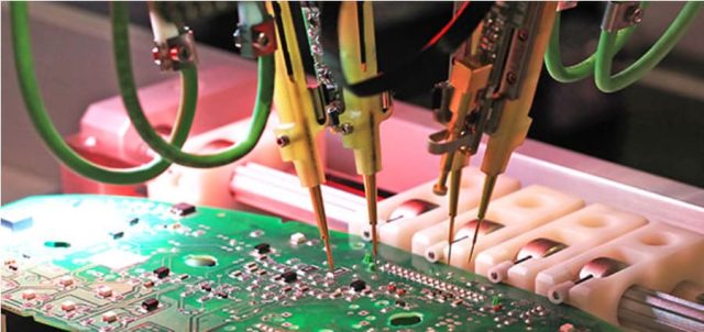
Custom probe card PCBs are widely used in:
-
Wafer-level functional testing
-
Parametric and DC testing
-
High-speed digital and RF wafer testing
-
Advanced node semiconductor validation
Each application demands precision and reliability.
Selecting a Custom Probe Card PCB Manufacturer
When choosing a custom probe card PCB supplier, consider:
-
Experience in semiconductor test PCB manufacturing
-
Capability for fine-line and high-density designs
-
Strong process control and traceability
-
Engineering collaboration during design and DFM review
An experienced partner reduces risk and improves test consistency.
Conclusion
The Custom Probe Card PCB is a mission-critical component in semiconductor wafer testing. By combining precise signal routing, mechanical stability, and advanced manufacturing control, these PCBs enable accurate and repeatable test results.
Working with a professional custom probe card PCB manufacturer ensures reliable performance throughout the entire testing lifecycle.
