In RF, microwave, and high-speed electronics testing, measurement accuracy depends not only on instruments but also on the quality of the test interface. A High Frequency Test PCB acts as the electrical bridge between the device under test and the measurement system, making its design and fabrication critical to reliable results.
Unlike standard production PCBs, high frequency test PCBs prioritize signal fidelity and repeatability over cost optimization.
The Role of High Frequency Test PCBs in Measurement Accuracy
High frequency testing exposes every weakness in a PCB design. Poor impedance control, unstable materials, or inconsistent manufacturing can introduce:
-
Return loss and reflections
-
Phase and amplitude errors
-
Inconsistent test data
A purpose-built high frequency test PCB minimizes these risks.
Design Priorities for High Frequency Test PCBs
Effective high frequency test PCB design focuses on:
-
Clean signal transitions
-
Stable reference planes
-
Minimal discontinuities
Routing discipline is often more important than routing density in test boards.
Material Stability Across Frequency and Temperature
High frequency test PCBs typically operate across wide temperature and frequency ranges. Stable materials help maintain:
-
Consistent dielectric constant
-
Low dissipation factor
-
Predictable impedance
Rogers, PTFE-based, and hybrid materials are commonly selected for this reason.
Impedance Consistency and Trace Geometry Control
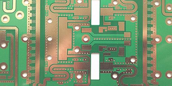
Unlike production boards that tolerate small variations, test PCBs demand:
-
Tight impedance tolerance
-
Uniform trace width and spacing
-
Controlled dielectric thickness
These factors directly influence measurement repeatability.
Managing Parasitics in Vias and Transitions
Vias, connectors, and layer transitions introduce parasitic effects that distort high frequency signals. High frequency test PCBs mitigate these effects by:
-
Using short signal paths
-
Eliminating unused via stubs
-
Adding ground stitching near RF transitions
Proper parasitic control improves correlation between simulations and measurements.
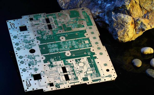
Manufacturing Consistency for Repeatable Testing
Repeatable test results require consistent manufacturing. Key fabrication controls include:
-
Precision etching
-
Accurate lamination thickness
-
Reliable via plating
Test boards often undergo stricter inspection than standard PCBs.
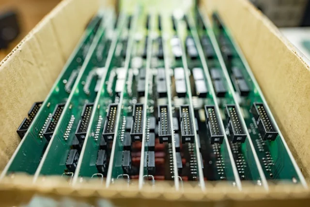
Common Applications of High Frequency Test PCBs
High frequency test PCBs are widely used in:
-
RF component characterization
-
Microwave module validation
-
5G and mmWave device testing
-
Automotive radar and antenna evaluation
Each application depends on predictable electrical behavior.
Selecting a High Frequency Test PCB Manufacturing Partner
When choosing a high frequency test PCB manufacturer, engineers should evaluate:
-
Experience with RF test boards
-
Material handling and stackup expertise
-
Electrical testing capability
-
Engineering feedback during DFM review
A knowledgeable partner reduces test uncertainty.
Conclusion
A High Frequency Test PCB is a critical measurement tool, not just a circuit carrier. Through disciplined design, stable materials, and precise manufacturing, these test boards enable accurate, repeatable RF and microwave measurements.
Working with an experienced high frequency test PCB supplier ensures that test data reflects true device performance rather than PCB-induced artifacts.
