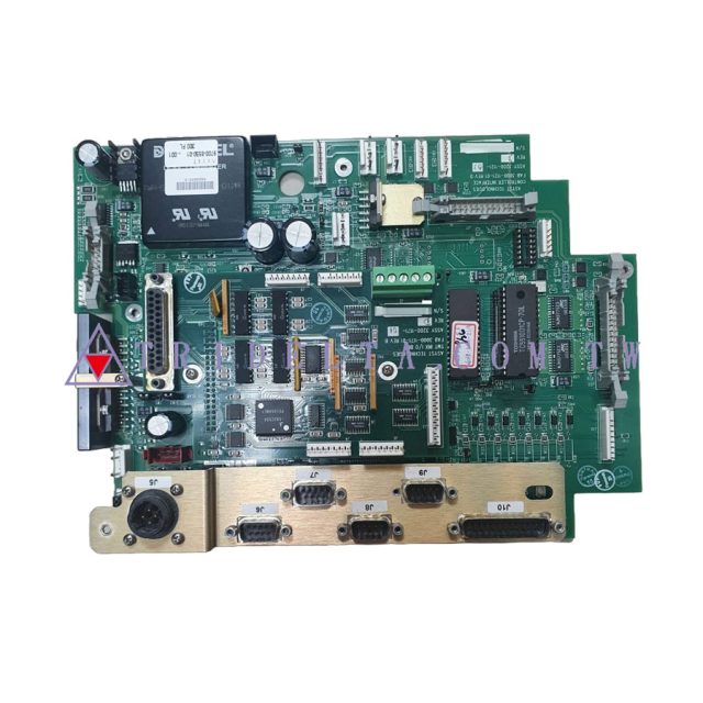
In semiconductor mass production, test throughput and consistency are just as important as accuracy. The Load Board PCB is a critical interface between automated test equipment (ATE) and packaged semiconductor devices, ensuring reliable electrical connection and repeatable test performance during high-volume production.
A well-designed Load Board PCB minimizes downtime, reduces false failures, and supports long-term production stability.
What Is a Load Board PCB?
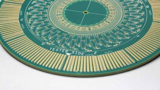
A Load Board PCB is a specialized printed circuit board used in final test and system-level test environments. It provides:
-
Electrical interconnection between ATE channels and DUT pins
-
Power delivery and grounding networks for packaged devices
-
Mechanical support for test sockets and fixtures
Load board PCBs are designed for durability and repeated use in production testing.
The Role of Load Board PCBs in Semiconductor Testing
Load board PCBs are typically used after wafer probing and package-level validation. Their main roles include:
-
Verifying device functionality in production conditions
-
Supporting high-speed and high-pin-count device testing
-
Enabling high-throughput automated testing
Reliability at this stage directly affects yield and cost.
Signal Integrity for High-Speed Load Board PCBs
High-speed digital and RF devices require precise signal control. Load board PCB designs incorporate:
-
Controlled impedance routing
-
Length matching for timing-critical signals
-
Clean return path and reference plane design
Good signal integrity ensures accurate test results at production speeds.
Power Integrity and Thermal Considerations
Production testing often involves high current and long test cycles. A Load Board PCB must provide:
-
Low-impedance power planes
-
Robust decoupling and bulk capacitance
-
Thermal stability under continuous operation
Stable power delivery reduces noise-induced test failures.
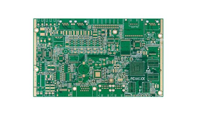
Supporting High Pin Count and Dense Routing
Modern IC packages often exceed hundreds or thousands of pins. Load board PCBs support:
-
Multilayer and HDI PCB structures
-
Fine-pitch breakout and via-in-pad technology
-
Optimized routing for dense pin maps
High-density capability enables full device coverage.
Mechanical Strength and Socket Integration
Load Board PCBs experience frequent socket insertions and mechanical stress. Reliable designs include:
-
Reinforced socket mounting areas
-
Tight flatness and coplanarity control
-
Warpage-resistant stackup design
Mechanical robustness ensures long-term test stability.
Material Selection for Load Board PCBs
Material choice affects both durability and electrical performance. Common options include:
-
High-Tg FR-4 for mechanical strength
-
Low-loss laminates for high-speed signals
-
Hybrid stackups for mixed-signal testing
Materials are selected based on device speed and test environment.
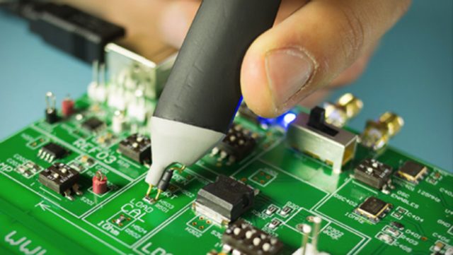
Manufacturing Precision and Quality Control
Consistency is critical for production testing. High-quality Load Board PCBs require:
-
Tight laminate thickness control
-
Accurate drilling, plating, and etching
-
Electrical and impedance verification
Manufacturing precision ensures consistent test performance across builds.
Typical Applications of Load Board PCBs
Load Board PCBs are widely used in:
-
Final test of logic and memory devices
-
Automotive and industrial IC production
-
High-speed communication and processor testing
-
System-level test (SLT) environments
Each application demands high reliability and repeatability.
Choosing a Load Board PCB Manufacturing Partner
When selecting a Load Board PCB manufacturer, consider:
-
Experience with high-volume semiconductor testing
-
High pin count and controlled impedance capability
-
Proven mechanical reliability in production use
-
Engineering support for complex socket integration
The right partner helps reduce downtime and test cost.
Conclusion
The Load Board PCB is a cornerstone of reliable semiconductor production testing. By ensuring strong signal integrity, stable power delivery, mechanical durability, and manufacturing consistency, a well-designed load board PCB enables efficient, repeatable, and scalable high-volume testing.
Partnering with an experienced Load Board PCB supplier is essential for long-term production success.
