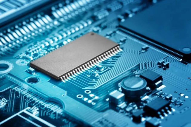
Semiconductor devices must pass multiple test stages before entering mass production and end-use applications. At every stage, the Semiconductor Test PCB plays a vital role in ensuring accurate measurement, stable operation, and repeatable test results. Whether used in wafer probing, package testing, or final system validation, a well-designed semiconductor test PCB directly impacts yield, reliability, and overall test efficiency.
What Is a Semiconductor Test PCB?
A Semiconductor Test PCB is a specialized printed circuit board designed to interface semiconductor devices with automated test equipment (ATE) or laboratory test systems. It supports:
-
Electrical signal routing between tester and DUT
-
Power delivery and grounding networks
-
Mechanical interfaces such as probes, sockets, or connectors
These PCBs are engineered specifically for test accuracy and durability.
The Role of Semiconductor Test PCBs in the Test Flow
Semiconductor test PCBs are used throughout the device lifecycle, including:
-
Wafer-level testing and characterization
-
Package-level functional and parametric testing
-
Final test and system-level validation
Each stage places unique electrical and mechanical demands on the test PCB.
Signal Integrity for High-Speed Semiconductor Testing
As semiconductor devices operate at higher speeds, maintaining signal integrity becomes increasingly critical. Semiconductor Test PCBs address this by:
-
Controlled impedance routing
-
Length matching for timing-sensitive signals
-
Optimized reference plane and return path design
These measures ensure accurate high-speed signal transmission.
Power Integrity and Noise Control
Stable power delivery is essential for reliable semiconductor testing. A well-designed Semiconductor Test PCB includes:
-
Low-impedance power planes
-
Strategic decoupling and bulk capacitance
-
Effective grounding strategies
Good power integrity minimizes false failures and test variation.
Supporting High Pin Count and Dense Interfaces
Modern ICs often feature hundreds or thousands of pins. Semiconductor test PCBs support:
-
High pin count routing
-
Multilayer and HDI PCB structures
-
Fine-pitch breakout and via-in-pad technology
Dense routing capability ensures complete device coverage.
Mechanical Reliability and Test Repeatability
Test PCBs experience repeated insertions and mechanical stress. To ensure long-term reliability, Semiconductor Test PCBs are designed with:
-
Reinforced socket or probe mounting areas
-
Tight flatness and coplanarity control
-
Warpage-resistant stackup structures
Mechanical stability directly impacts test consistency.
Material and Stackup Considerations
Material selection depends on test requirements. Semiconductor test PCBs commonly use:
-
High-Tg FR-4 for durability
-
Low-loss laminates for high-speed or RF testing
-
Hybrid stackups for mixed-signal devices
Material stability ensures consistent performance across test conditions.
Manufacturing Precision and Quality Assurance
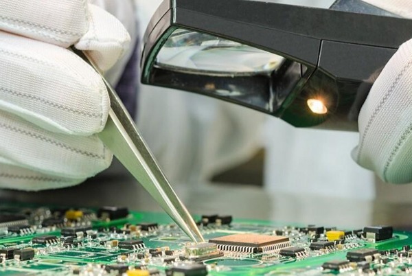
Because test results depend heavily on PCB consistency, Semiconductor Test PCBs require:
-
Tight manufacturing tolerances
-
Accurate drilling, plating, and etching
-
Electrical testing and impedance verification
Strong quality control ensures repeatable test performance.
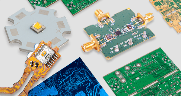
Typical Applications of Semiconductor Test PCBs
Semiconductor Test PCBs are widely used in:
-
Logic and memory device testing
-
Automotive and industrial IC validation
-
RF, mixed-signal, and power device testing
-
High-reliability and safety-critical applications
Each application demands precision and reliability.
Choosing a Semiconductor Test PCB Manufacturing Partner
When selecting a Semiconductor Test PCB manufacturer, consider:
-
Experience across multiple semiconductor test stages
-
High pin count and controlled impedance capability
-
Proven reliability in production test environments
-
Engineering support for complex test requirements
A knowledgeable partner helps reduce test risk and accelerate validation.
Conclusion
The Semiconductor Test PCB is a foundational element of reliable semiconductor testing. By supporting signal integrity, power stability, mechanical durability, and manufacturing precision, a high-quality semiconductor test PCB ensures accurate results from wafer validation to final device qualification.
Partnering with an experienced Semiconductor Test PCB supplier is essential for consistent, high-yield semiconductor testing.
