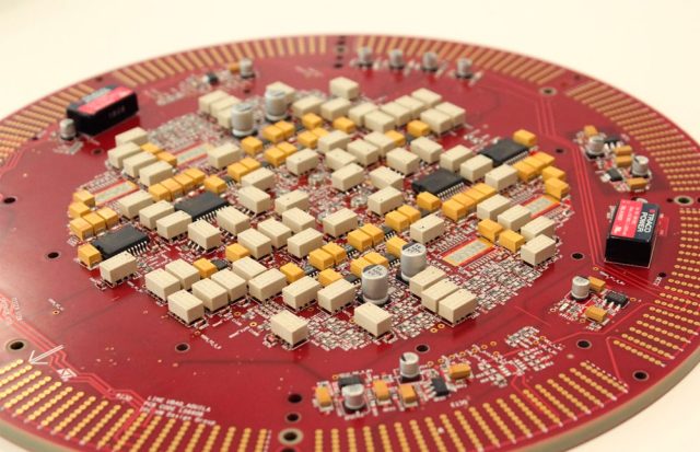
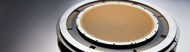
Wafer-level testing is one of the most demanding stages in semiconductor manufacturing. At this level, accuracy, repeatability, and mechanical precision are critical. The Probe Card PCB serves as the core platform that connects automated test equipment (ATE) to semiconductor wafers, enabling precise electrical contact and reliable signal transmission during wafer probing.
A high-quality Probe Card PCB ensures stable testing performance while minimizing measurement errors and yield loss.
What Is a Probe Card PCB?
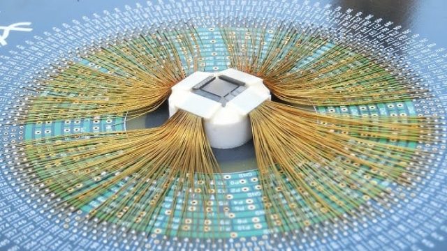
A Probe Card PCB is a specialized printed circuit board used in wafer probing systems. It supports:
-
Probe needles or MEMS probe structures
-
High-density signal routing between probes and ATE
-
Power and ground distribution for wafer-level testing
Probe card PCBs are designed to operate with extreme precision at micron-level contact pitches.
Why Probe Card PCB Design Is Critical
Unlike final test boards, probe card PCBs must handle:
-
Ultra-fine pitch contact points
-
Extremely tight planarity requirements
-
Frequent mechanical movement and contact cycles
Any instability in the Probe Card PCB can result in poor contact, signal distortion, or false test results.
High-Density Signal Routing and Impedance Control
Probe card PCBs often support thousands of test channels. Key design features include:
-
High-density routing with microvias and fine traces
-
Controlled impedance signal paths for high-speed testing
-
Optimized return path design
These features ensure accurate signal transmission from wafer to tester.
Mechanical Stability and Planarity Control
Mechanical precision is critical for consistent probe contact. A Probe Card PCB must provide:
-
Excellent flatness and coplanarity
-
Balanced multilayer stackup to prevent warpage
-
Reinforced structures to support probe assemblies
Stable mechanics directly impact test yield and repeatability.
Material Selection for Probe Card PCBs
Material choice affects both electrical and mechanical performance. Common materials include:
-
High-Tg FR-4 for structural stability
-
Low-CTE laminates to reduce thermal expansion
-
Hybrid stackups for mixed-signal probing
Material stability ensures reliable performance across temperature variations.
Signal Integrity at High Frequencies
As test speeds increase, signal integrity becomes more challenging. Probe card PCBs address this by:
-
Minimizing signal path length
-
Reducing parasitic capacitance and inductance
-
Controlling impedance transitions between probes and PCB traces
Clean signal transmission improves measurement accuracy.
Power and Ground Distribution
Stable power delivery is essential for accurate wafer testing. Probe card PCBs incorporate:
-
Dedicated power and ground planes
-
Localized decoupling near probe interfaces
-
Low-noise grounding strategies
Proper power design prevents measurement instability.
Manufacturing Precision and Quality Control
Probe card PCBs demand extremely tight manufacturing tolerances, including:
-
Precise drilling and via alignment
-
Controlled copper thickness and trace geometry
-
Electrical and dimensional inspection
Manufacturing quality directly affects probing accuracy.
Typical Applications of Probe Card PCBs
Probe Card PCBs are widely used in:
-
Wafer-level parametric testing
-
Logic and memory device probing
-
RF and mixed-signal wafer testing
-
Advanced packaging and chiplet testing
Each application requires exceptional precision.
Choosing a Probe Card PCB Manufacturing Partner
When selecting a Probe Card PCB manufacturer, consider:
-
Experience with wafer-level test PCBs
-
High-density and fine-pitch manufacturing capability
-
Strong control of flatness and tolerances
-
Engineering support for complex probe structures
The right partner ensures stable probing performance.
Conclusion
The Probe Card PCB is a critical component in wafer-level semiconductor testing. By combining high-density routing, controlled impedance, mechanical stability, and manufacturing precision, a well-designed probe card PCB enables accurate, repeatable, and high-yield wafer testing.
Partnering with an experienced Probe Card PCB supplier is essential for reliable semiconductor test operations.
