Automated Test Equipment (ATE) is the backbone of modern semiconductor validation and mass production. At the center of every ATE system is the ATE Test PCB, which directly affects test accuracy, yield stability, and long-term reliability. A well-engineered ATE test PCB ensures that measured performance reflects the device under test—not limitations of the test hardware.
What Is an ATE Test PCB?
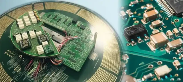
An ATE Test PCB is a specialized printed circuit board used as the electrical interface between an ATE system and the device under test (DUT). It provides:
-
Signal routing between tester channels and DUT pins
-
Power distribution and grounding networks
-
Mechanical support for sockets or probe interfaces
ATE test PCBs are designed for high reliability and repeated use in production environments.
Why ATE Test PCB Design Is Critical
ATE systems operate at high speeds and high pin counts. Poor PCB design can result in:
-
Signal integrity degradation
-
Power noise and ground bounce
-
Intermittent contact and false failures
A high-quality ATE Test PCB minimizes these risks and improves test consistency.
Signal Integrity in ATE Test PCBs
Maintaining clean signal transmission is essential. ATE test PCBs incorporate:
-
Controlled impedance routing
-
Length matching for timing-critical signals
-
Optimized return path and reference plane design
These measures ensure accurate high-speed measurements.
Power Integrity and Grounding Strategy
Power delivery directly affects test stability. An ATE Test PCB must support:
-
Low-impedance power planes
-
Proper decoupling and bulk capacitance
-
Isolated ground regions where required
Stable power minimizes noise-induced test errors.
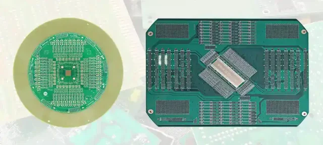
High Pin Count and Dense Routing Challenges
Modern devices often require thousands of test connections. ATE test PCBs address this with:
-
Multilayer and HDI PCB structures
-
Fine-pitch via and trace technology
-
Optimized breakout strategies
High-density routing enables reliable access to all DUT pins.
Mechanical Reliability and Socket Integration
ATE test PCBs are subject to frequent socket insertions. Reliable designs include:
-
Reinforced socket mounting areas
-
Tight flatness and coplanarity control
-
Warpage-resistant stackup design
Mechanical stability ensures consistent electrical contact over time.
Material Selection for ATE Test PCBs
Material choice impacts both electrical and mechanical performance. Common materials include:
-
High-Tg FR-4 for durability
-
Low-loss laminates for high-speed signals
-
Hybrid stackups for mixed-signal applications
Materials are selected based on test speed and environment.
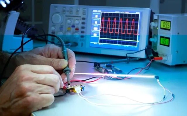
Manufacturing Precision and Quality Control
Because ATE test PCBs are used in production, consistency is essential. Key manufacturing controls include:
-
Tight laminate thickness tolerances
-
Accurate drilling and plating
-
Electrical testing and impedance verification
Quality control ensures repeatable test performance.
Typical Applications of ATE Test PCBs
ATE Test PCBs are widely used in:
-
Semiconductor wafer and final test
-
System-level test (SLT)
-
Automotive and industrial IC testing
-
High-speed logic and memory devices
Each application demands high reliability and precision.
Choosing an ATE Test PCB Manufacturing Partner
When selecting an ATE Test PCB manufacturer, consider:
-
Experience with ATE platforms
-
High pin count and controlled impedance capability
-
Proven reliability in production environments
-
Engineering support and fast turnaround
The right partner reduces test risk and downtime.
Conclusion
The ATE Test PCB plays a critical role in ensuring accurate, repeatable, and scalable semiconductor testing. Through careful signal and power integrity design, mechanical reliability, and precise manufacturing, a well-designed ATE test PCB supports stable test results from development through mass production.
Partnering with an experienced ATE Test PCB supplier is essential for long-term testing success.
