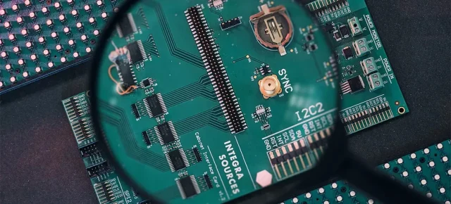
In semiconductor manufacturing, testing is not a single step—it is a continuous process that spans wafer probing, device validation, system-level testing, and mass production. At the core of this process lies the Semiconductor Test PCB, a specialized printed circuit board designed to deliver consistent electrical performance across every test stage.
A well-designed Semiconductor Test PCB directly impacts test accuracy, yield stability, and time-to-market for advanced IC products.
What Is a Semiconductor Test PCB?
A Semiconductor Test PCB is a category of high-performance PCB used to electrically interface test equipment with semiconductor devices under various test conditions. It acts as the physical and electrical bridge between:
-
Automated Test Equipment (ATE)
-
Devices Under Test (DUTs)
-
Test sockets, probe cards, or fixtures
Unlike standard application PCBs, semiconductor test PCBs prioritize measurement integrity, repeatability, and durability.
Why Semiconductor Test PCBs Are Critical
Inaccurate or unstable test boards can lead to:
-
False test failures
-
Reduced test yield
-
Inconsistent parametric data
-
Undetected device defects
A professionally manufactured Semiconductor Test PCB ensures that each device is evaluated under controlled and repeatable electrical conditions.
Supporting Multiple Test Phases
Semiconductor test PCBs are used throughout the IC lifecycle:
-
Wafer-level test (in combination with probe cards)
-
Engineering validation test (EVT/DVT)
-
Final production test
-
System-level test (SLT)
Each phase places different demands on PCB design, making flexibility and stability essential.
Signal Integrity in Semiconductor Test PCBs
As IC speeds continue to increase, signal integrity becomes a defining requirement. Effective semiconductor test PCB designs incorporate:
-
Controlled impedance routing
-
Optimized trace length matching
-
Proper return path and reference plane design
These measures reduce signal distortion, jitter, and crosstalk during high-speed testing.
Power Integrity and Noise Control
Semiconductor devices are highly sensitive to power fluctuations. A high-quality Semiconductor Test PCB ensures:
-
Low-impedance power distribution networks
-
Strategic decoupling capacitor placement
-
Strong grounding to minimize noise coupling
Stable power delivery is essential for reliable parametric and functional testing.
High Pin Count and Complex Interfacing
Modern ICs often require hundreds or thousands of test connections. Semiconductor test PCBs must support:
-
High pin count layouts
-
Fine-pitch routing and HDI structures
-
Mixed-signal and multi-voltage domains
Precision routing and layer stackup design are critical to maintain electrical performance.
Mechanical Reliability and Long-Term Stability
Repeated test cycles place mechanical stress on semiconductor test PCBs through sockets and connectors. Long-term reliability depends on:
-
Excellent PCB flatness
-
Reinforced high-stress areas
-
Balanced multilayer stackups
Mechanical stability ensures consistent contact quality over extended production runs.
Materials and Stackup Optimization
Material selection for semiconductor test PCBs focuses on stability and durability:
-
High-Tg FR-4 for structural reliability
-
Low-loss laminates for high-speed signal paths
-
Hybrid stackups for mixed-frequency testing
These materials help maintain consistent electrical behavior across temperature and time.
Manufacturing Consistency Matters
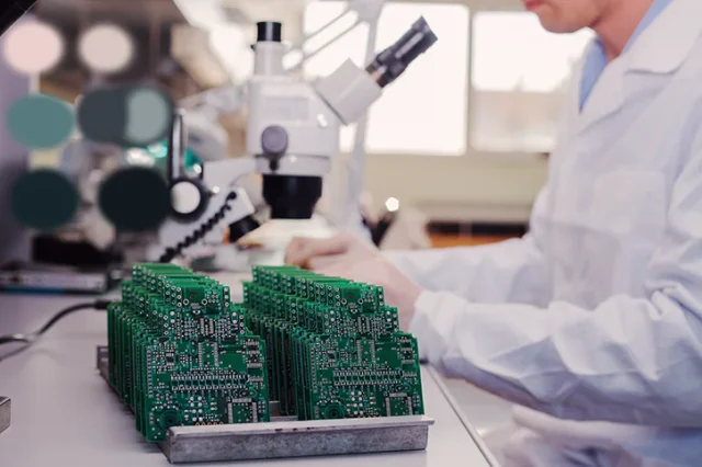
Unlike one-off prototypes, semiconductor test PCBs must perform consistently across multiple builds. This requires:
-
Tight process control
-
Precise layer registration
-
Reliable via formation and plating
-
Electrical and impedance verification
Manufacturing variation directly affects test accuracy.
Typical Applications of Semiconductor Test PCBs
Semiconductor test PCBs are widely used in:
-
Logic and memory device testing
-
Automotive and industrial IC qualification
-
RF and mixed-signal semiconductor testing
-
Power management and analog device validation
Each application demands stable, repeatable test performance.
Choosing the Right Semiconductor Test PCB Supplier
When selecting a Semiconductor Test PCB manufacturer, consider:
-
Experience in semiconductor test hardware
-
High pin count and controlled impedance capability
-
Strong quality and traceability systems
-
Engineering support for fast iteration
A reliable supplier helps maintain consistent test results throughout production.
Conclusion
The Semiconductor Test PCB is a fundamental component in ensuring accurate and reliable IC testing across the entire semiconductor lifecycle. By combining signal integrity, power stability, mechanical reliability, and manufacturing consistency, a high-quality semiconductor test PCB supports higher yields, faster validation, and dependable mass production.
Choosing an experienced Semiconductor Test PCB supplier is essential for long-term test success.
