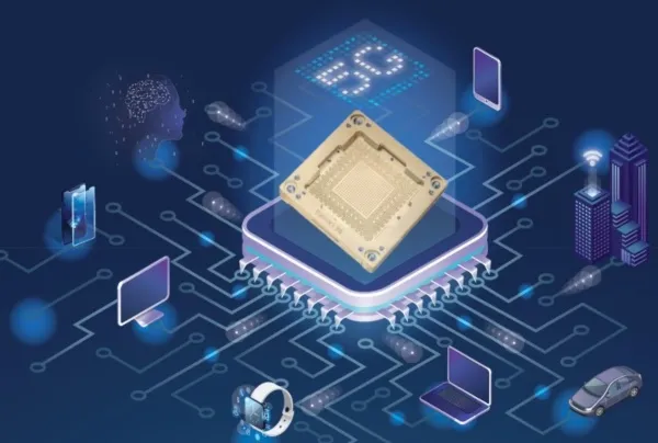
In semiconductor testing environments, stable electrical contact is just as important as tester accuracy. Even the most advanced ATE systems cannot deliver consistent results without a reliable interface between the device under test (DUT) and the test platform. The test socket PCB serves as this critical interface, directly influencing contact reliability, signal integrity, and test yield.
A professionally designed test socket PCB ensures repeatable performance across thousands of insertion cycles in high-volume testing.
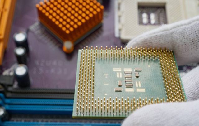
What Is a Test Socket PCB?
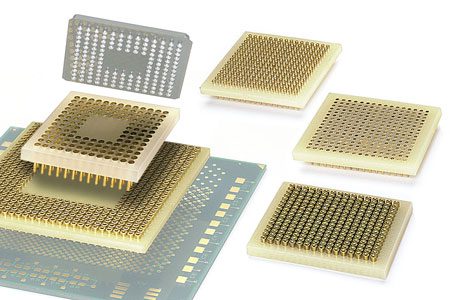
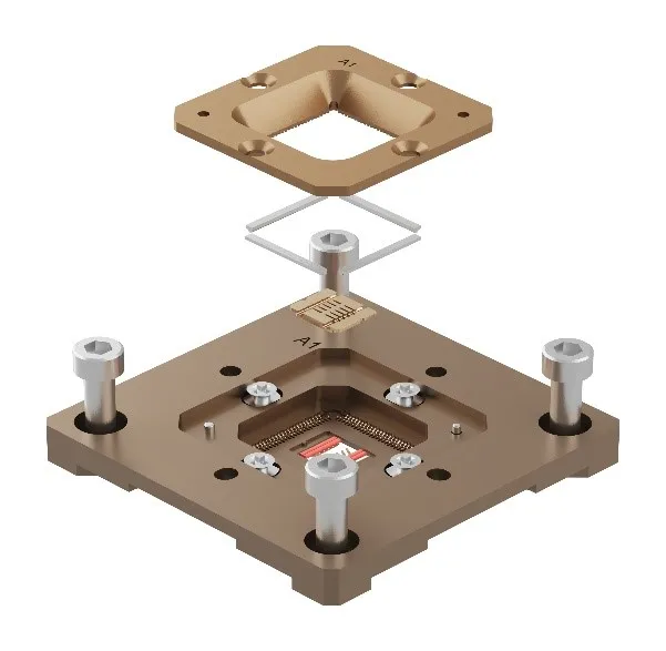
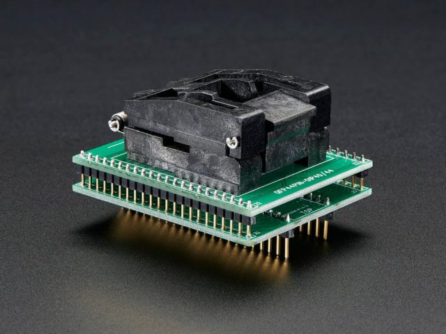
A test socket PCB is a specialized printed circuit board used to mount and support test sockets in IC testing systems. It electrically connects the DUT pins to the ATE or load board while maintaining precise alignment and stable electrical paths.
Unlike standard PCBs, test socket PCBs must withstand:
-
Repeated mechanical insertion and removal
-
High pin-count connectivity
-
Continuous electrical stress during testing
These requirements make test socket PCB design and manufacturing highly specialized.
Why Test Socket PCB Quality Is Critical
Poor-quality test socket PCBs can lead to:
-
Unstable contact resistance
-
Signal distortion and timing errors
-
Intermittent test failures
-
Reduced socket and DUT lifespan
A high-quality test socket PCB minimizes these risks by providing a stable mechanical and electrical foundation for the socket.
Signal Integrity Considerations
As IC speeds continue to increase, test socket PCB design must address:
-
Controlled impedance routing for high-speed signals
-
Short and symmetrical signal paths
-
Proper grounding to reduce noise and crosstalk
Maintaining consistent electrical characteristics across all channels ensures accurate and repeatable test results.
Mechanical Strength and Flatness Control
Test socket PCBs experience constant mechanical stress. Critical mechanical design elements include:
-
Excellent PCB flatness for uniform socket contact
-
Reinforced mounting areas
-
Stable materials to resist warpage
Mechanical reliability directly affects contact consistency and test stability.
Materials Used in Test Socket PCBs
Material selection balances durability and electrical performance:
-
High-Tg FR-4 for structural strength
-
Low-loss laminates for high-speed testing
-
Hybrid stackups for mixed-signal applications
Stable material properties help maintain performance over long test cycles.
Manufacturing Precision and Quality Control
Producing a reliable test socket PCB requires tight process control:
-
Accurate drilling and via plating
-
Consistent laminate thickness
-
Precise layer alignment
-
Electrical testing for continuity and impedance
Manufacturing consistency ensures each board performs identically in production.
Applications of Test Socket PCBs
Test socket PCBs are widely used in:
-
IC final testing
-
Burn-in and reliability testing
-
Automotive semiconductor validation
-
Consumer and industrial electronics testing
Each application demands high reliability and repeatability.
Choosing the Right Test Socket PCB Manufacturer
When selecting a test socket PCB manufacturer, consider:
-
Experience with semiconductor test PCBs
-
Ability to handle high pin-count designs
-
Proven mechanical and electrical quality control
-
Support for quick-turn and volume production
A reliable partner helps reduce downtime and improve overall test efficiency.
Conclusion
The test socket PCB is a vital component in semiconductor testing, ensuring reliable electrical contact and stable signal transmission. Through careful design, robust materials, and precise manufacturing, high-quality test socket PCBs enable accurate testing, higher yield, and long-term reliability.
Choosing an experienced test socket PCB supplier ensures consistent performance throughout the entire testing process.
