As semiconductor devices continue to scale in complexity and pin density, wafer-level testing requires extreme accuracy and repeatability. At the core of this process lies the probe card PCB, a critical interface that connects automated test equipment (ATE) to semiconductor wafers.
A high-quality probe card PCB directly determines signal integrity, contact accuracy, and long-term test stability.
What Is a Probe Card PCB?
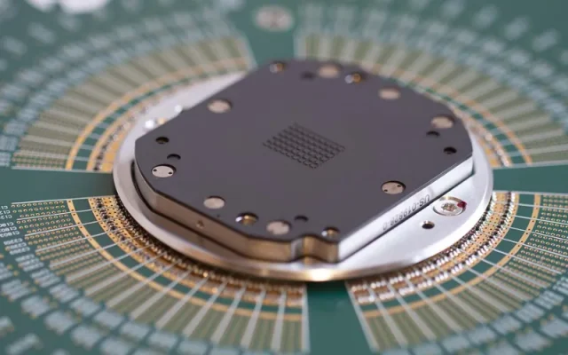
A probe card PCB is a specialized printed circuit board used in probe cards for semiconductor wafer testing. It provides electrical routing between probe needles (or MEMS probes) and the ATE system, ensuring precise signal transmission during wafer probing.
Unlike standard PCBs, probe card PCBs are designed to support:
-
Extremely fine pitch interconnections
-
High pin counts
-
High-speed and mixed-signal testing
-
Mechanical stability under repeated contact cycles
Why Probe Card PCB Precision Is Critical
Probe card testing occurs before IC packaging, where margins for error are minimal. Any variation in the probe card PCB can lead to:
-
Signal distortion or noise
-
Inaccurate test results
-
Increased wafer scrap rates
-
Reduced probe card lifespan
Precision PCB fabrication is essential to maintain test accuracy across millions of probe touchdowns.
Key Design Requirements for Probe Card PCBs
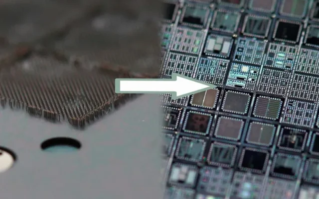
High-Density Routing Capability
Modern probe card PCBs must support:
-
Fine line / space geometries
-
Microvias and via-in-pad designs
-
Multilayer stackups for dense signal routing
High-density interconnection is necessary to accommodate advanced semiconductor nodes.
Controlled Impedance and Signal Integrity
High-speed wafer testing demands:
-
Controlled impedance traces
-
Stable dielectric materials
-
Consistent layer thickness
This ensures accurate transmission of high-speed digital and RF test signals.
Mechanical Stability and Flatness
Probe card PCBs must maintain:
-
Excellent planarity
-
Minimal warpage
-
Structural rigidity under thermal and mechanical stress
Flatness directly impacts probe-to-pad contact accuracy.
Materials Used in Probe Card PCBs
Depending on test requirements, probe card PCBs may use:
-
High-Tg FR-4 for mechanical strength
-
Low-loss laminates for high-speed or RF testing
-
Specialized materials with low CTE for dimensional stability
Material selection balances electrical performance with mechanical durability.
Manufacturing Challenges of Probe Card PCBs
Producing a reliable probe card PCB requires advanced manufacturing capabilities:
-
Tight tolerance drilling and plating
-
Precise layer alignment and registration
-
Uniform copper thickness control
-
Strict cleanliness and contamination control
Even small process deviations can affect test accuracy.
Quality Control and Testing
Professional probe card PCB manufacturers implement:
-
AOI and electrical testing
-
Impedance verification
-
Dimensional and flatness inspection
-
Process traceability
These controls ensure consistency from prototype to volume production.
Applications of Probe Card PCBs
Probe card PCBs are widely used in:
-
Logic IC wafer testing
-
Memory device testing
-
Mixed-signal and analog IC testing
-
RF and high-speed semiconductor devices
Each application demands high precision and repeatable performance.
Choosing the Right Probe Card PCB Manufacturer
When selecting a supplier for probe card PCB fabrication, consider:
-
Experience with semiconductor test PCBs
-
HDI and fine-pitch manufacturing capability
-
Controlled impedance expertise
-
Proven quality and reliability systems
A reliable partner ensures stable test performance and long probe card service life.
Conclusion
The probe card PCB is a foundational element in semiconductor wafer testing, directly influencing test accuracy, yield, and efficiency. Through precision design, advanced materials, and tightly controlled manufacturing processes, high-quality probe card PCBs support reliable, repeatable semiconductor testing at scale.
Choosing an experienced probe card PCB manufacturer is essential for achieving consistent test results and maximizing probe card performance.
