For high-speed digital and RF electronic systems, signal integrity is one of the most critical design challenges. A controlled impedance PCB prototype plays a key role in validating design assumptions, manufacturing tolerances, and electrical performance before moving into mass production.
Building controlled impedance into the prototype stage significantly reduces technical and production risk.
What Is a Controlled Impedance PCB Prototype?
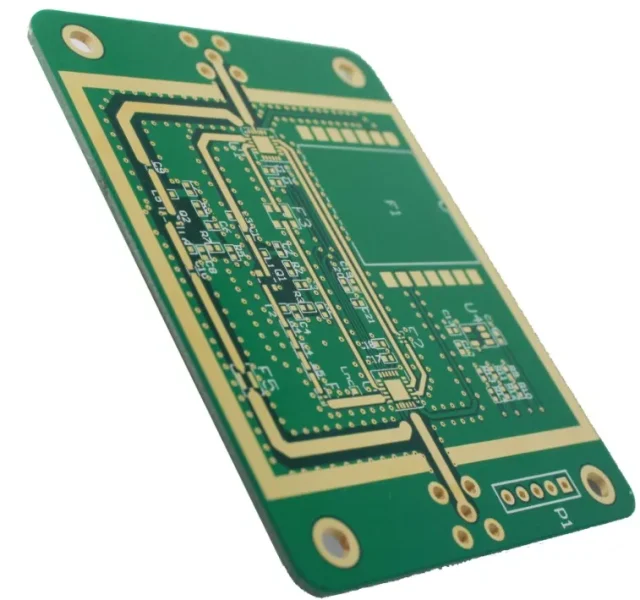
A controlled impedance PCB prototype is a prototype PCB fabricated with specific impedance targets—such as 50Ω single-ended or 90Ω differential—achieved through precise control of stackup structure, dielectric thickness, and trace geometry.
Unlike standard prototypes, these boards are designed and manufactured to replicate production-level impedance behavior.
Why Impedance Control Matters in Prototyping
During the prototype phase, uncontrolled impedance can lead to:
-
Signal reflection and eye diagram distortion
-
Increased crosstalk and EMI
-
Inconsistent test results between builds
A controlled impedance PCB prototype ensures that measured performance accurately reflects the final product design.
Key Validation Goals of a Controlled Impedance PCB Prototype
A professional controlled impedance PCB prototype helps engineers:
-
Verify stackup assumptions and material behavior
-
Validate impedance targets through TDR testing
-
Evaluate signal integrity under real operating conditions
-
Confirm manufacturing consistency and yield potential
These validations prevent costly redesigns later.
Stackup Design and Material Selection
Accurate impedance control begins with proper stackup planning. Controlled impedance PCB prototypes often use:
-
Defined dielectric thickness and copper weights
-
Low-loss materials for high-speed or RF signals
-
Consistent prepreg and core combinations
Working closely with the PCB manufacturer during stackup design is critical.
Manufacturing Considerations for Impedance-Controlled Prototypes
Producing a reliable controlled impedance PCB prototype requires:
-
Tight etching tolerance control
-
Stable lamination processes
-
Copper roughness management
-
In-process and final impedance testing
These manufacturing controls ensure prototype results are repeatable.
Typical Applications of Controlled Impedance PCB Prototypes
Controlled impedance PCB prototypes are widely used in:
-
High-speed digital interfaces (PCIe, USB, Ethernet)
-
RF and microwave circuits
-
5G and mmWave communication modules
-
Automotive radar and ADAS electronics
-
High-speed data processing systems
Each application depends on accurate signal transmission.
From Controlled Impedance Prototype to Production
A successful prototype should transition smoothly into production. This requires:
-
Consistent materials and stackups
-
Documented impedance performance
-
Scalable manufacturing processes
Partnering with an experienced manufacturer ensures production boards match prototype performance.
Conclusion
A controlled impedance PCB prototype is an essential step in validating high-speed and RF designs. By confirming impedance accuracy, signal integrity, and manufacturing feasibility early, engineers can reduce development risk, shorten time-to-market, and ensure stable performance in mass production.
Working with a manufacturer experienced in controlled impedance PCB prototyping ensures your design moves confidently from concept to production.
