As data rates and operating frequencies continue to increase, maintaining signal integrity becomes a critical design challenge. A controlled impedance PCB prototype allows engineers to verify impedance accuracy, minimize signal reflection, and validate high-speed or RF performance before entering mass production.
By prototyping controlled impedance PCBs early, design risks are reduced and product reliability is significantly improved.
What Is a Controlled Impedance PCB Prototype?
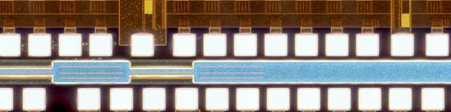
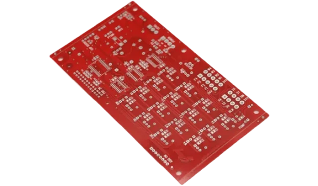
A controlled impedance PCB prototype is a prototype PCB manufactured with precisely defined trace geometry, dielectric thickness, and material properties to meet specific impedance targets such as 50Ω, 90Ω, or 100Ω.
These prototypes are commonly used for:
-
High-speed digital interfaces
-
RF and microwave circuits
-
Differential pair routing
-
High-frequency communication modules
Why Controlled Impedance PCB Prototyping Is Essential
Early Signal Integrity Verification
Controlled impedance PCB prototypes ensure trace impedance matches design targets, reducing reflection, jitter, and signal loss.
Stackup and Material Validation
Prototyping verifies real-world performance of selected materials such as FR-4, Rogers, Taconic, or hybrid stackups.
Reduced Design Iterations
Identifying impedance issues early prevents costly redesigns during volume production.
Faster Time-to-Market
Accurate prototypes accelerate design validation and product launch schedules.
Key Design Elements for Controlled Impedance PCB Prototypes
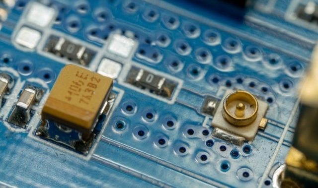
A professional controlled impedance PCB prototype process includes:
-
Stackup simulation and impedance calculation
-
Precise control of trace width, spacing, and dielectric thickness
-
Low-loss material selection for high-frequency signals
-
Differential pair length and skew control
These elements are critical to achieving consistent impedance performance.
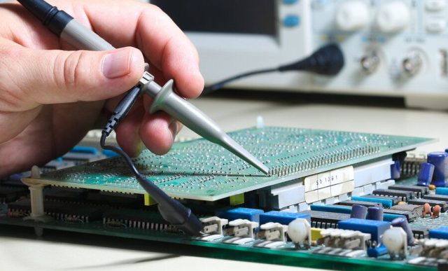
Manufacturing and Testing of Controlled Impedance PCB Prototypes
A reliable manufacturer provides:
-
Tight process control during fabrication
-
Controlled impedance tolerance (±10%, ±5%, or tighter)
-
TDR impedance testing and reporting
-
Electrical testing and visual inspection
Testing ensures the prototype meets design and performance expectations.
Applications of Controlled Impedance PCB Prototypes
Controlled impedance PCB prototypes are widely used in:
-
High-speed networking and data communication equipment
-
RF front-end and wireless modules
-
5G, mmWave, and automotive radar systems
-
Industrial and embedded electronics
Each application relies on precise impedance to maintain signal integrity.
Prototype to Mass Production Transition
A professional controlled impedance PCB prototype supplier supports:
-
Rapid prototyping with short lead times
-
DFM feedback for manufacturability
-
Consistent impedance control for volume production
-
Smooth scaling from prototype to mass production
This ensures prototype performance accurately represents production results.
How to Choose a Controlled Impedance PCB Prototype Partner
When selecting a controlled impedance PCB prototype manufacturer, consider:
-
Experience with high-speed and RF PCB designs
-
Impedance modeling and testing capability
-
Material expertise and stackup flexibility
-
Prototype turnaround time and engineering support
The right partner minimizes risk and ensures design success.
Conclusion
A controlled impedance PCB prototype is essential for validating signal integrity in high-speed and high-frequency electronic designs. By verifying impedance accuracy, stackup performance, and material behavior early in development, engineers can confidently move from prototype to mass production.
Partnering with an experienced controlled impedance PCB prototype manufacturer ensures reliable performance, reduced development risk, and faster time-to-market.
