As the Internet of Things (IoT) expands, high-frequency wireless devices require compact, reliable, and high-performance PCBs. A high frequency IoT PCB prototype allows engineers to validate RF performance, signal integrity, and overall design functionality before moving to mass production.
Prototyping high-frequency IoT PCBs enables early detection of design issues, optimization of stackups, and verification of controlled impedance in wireless modules, sensors, and communication devices.
What Is a High Frequency IoT PCB Prototype?
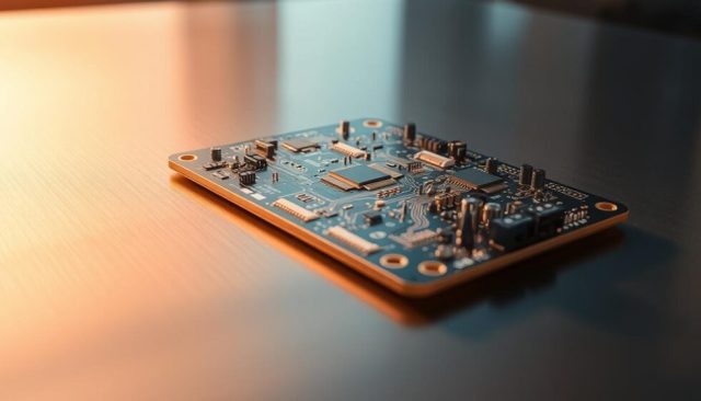
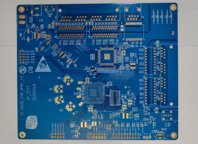
A high frequency IoT PCB prototype is a PCB manufactured with specialized low-loss materials, precise trace geometries, and controlled impedance to support high-speed and RF operation in IoT devices.
These prototypes are typically used in:
-
Wi-Fi, BLE, Zigbee, LoRa, and 5G IoT modules
-
RF front-end circuits and antenna connections
-
Wireless sensor networks and industrial IoT devices
-
Wearable IoT devices
Why High Frequency IoT PCB Prototyping Is Critical
Early Validation of Signal Integrity
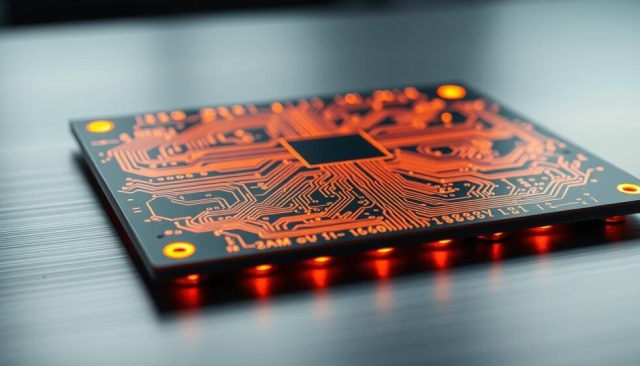
High-frequency IoT PCBs require careful impedance and trace design. Prototyping ensures minimal signal reflection and insertion loss.
Material and Stackup Verification
Low-loss laminates like Rogers, Taconic, or PTFE-based materials are verified during the prototype stage to ensure stable RF performance.
Rapid Design Iteration
Prototypes allow engineers to test, refine, and optimize designs before committing to large-scale production.
Reduced Time-to-Market
By identifying potential issues early, high frequency IoT PCB prototypes accelerate development cycles and minimize costly redesigns.
Materials and Design Considerations
Professional high frequency IoT PCB prototype services support:
-
Low-loss laminates for RF and high-speed signals
-
Controlled impedance design for antennas and RF paths
-
Fine-line trace capabilities for compact IoT devices
-
Multilayer PCB stackups to integrate multiple functions in small footprints
Correct material and stackup choices are essential for reliable IoT performance.
Prototype Manufacturing and Testing
A reliable high frequency IoT PCB prototype manufacturer provides:
-
Small batch prototyping with quick turnaround
-
Controlled impedance fabrication (±5% or tighter)
-
RF and electrical testing to verify functionality
-
DFM feedback and optimization for mass production
These processes ensure prototypes accurately reflect production performance.
Applications of High Frequency IoT PCB Prototypes

High frequency IoT PCB prototypes are used in:
-
Smart home devices (sensors, gateways, and controllers)
-
Industrial IoT modules and wireless automation systems
-
Wearable devices and medical monitoring equipment
-
5G IoT modules and high-speed RF transceivers
Prototyping ensures reliable performance in all these applications.
Choosing a Partner for High Frequency IoT PCB Prototypes
When selecting a high frequency IoT PCB prototype partner, consider:
-
Experience with RF and high-speed IoT PCBs
-
Controlled impedance design and testing capabilities
-
Material selection expertise for low-loss laminates
-
Rapid prototyping and scalable production support
The right partner ensures that prototypes provide accurate feedback for design refinement and mass production readiness.
Conclusion
A high frequency IoT PCB prototype is essential for developing reliable, high-performance wireless and IoT devices. By leveraging low-loss materials, precise impedance control, and RF testing, engineers can validate designs early, optimize performance, and accelerate time-to-market.
Partnering with an experienced high frequency IoT PCB prototype manufacturer ensures accurate, reliable, and production-ready prototypes for next-generation IoT applications.
