As digital speeds and operating frequencies continue to increase, maintaining signal integrity has become one of the biggest challenges in PCB design. A controlled impedance PCB prototype is a critical step in validating transmission line performance before mass production. By accurately controlling impedance during prototyping, engineers can reduce signal reflection, minimize loss, and ensure stable system operation in high-speed and RF designs.
What Is a Controlled Impedance PCB Prototype?
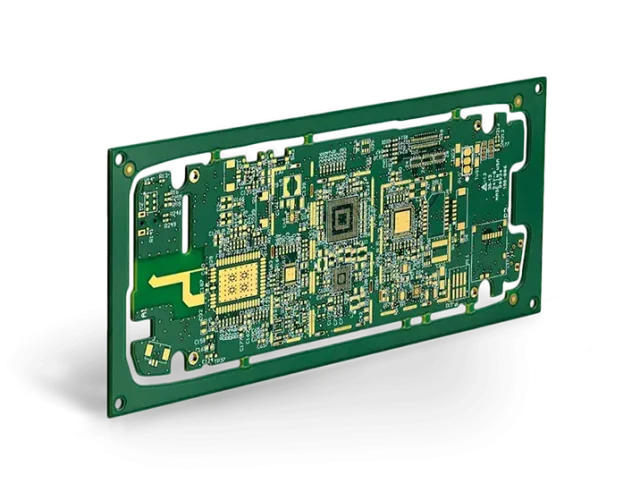
A controlled impedance PCB prototype is a low-volume PCB built with precisely defined impedance characteristics, typically for high-speed digital or RF applications. Common impedance targets include 50Ω single-ended, 90Ω and 100Ω differential pairs.
These prototypes are used to:
-
Verify impedance accuracy
-
Validate signal integrity
-
Test high-speed and RF performance
-
Identify design or stack-up issues early
Why Controlled Impedance Matters in PCB Prototyping
Impedance mismatches can cause:
-
Signal reflection and distortion
-
Eye diagram degradation
-
Increased EMI and crosstalk
-
System instability at high speeds
A controlled impedance PCB prototype allows engineers to confirm that the design meets electrical requirements before scaling to production.
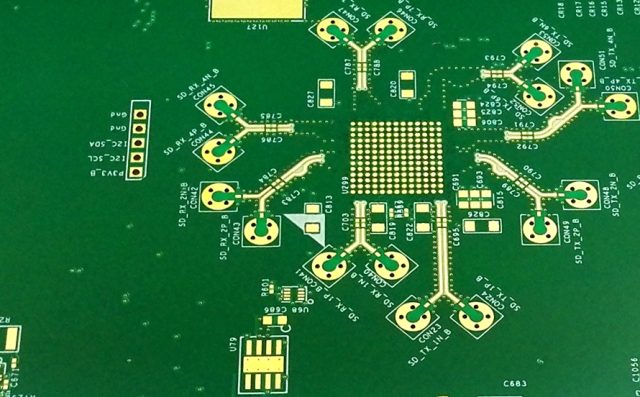
Key Elements of Controlled Impedance PCB Prototypes
Stack-Up Design and Simulation
Accurate stack-up planning is essential. Controlled impedance PCB prototypes rely on:
-
Precise dielectric thickness
-
Stable dielectric constant (Dk)
-
Controlled copper thickness
Simulation tools are often used to predict impedance before fabrication.
Material Selection
Material choice directly impacts impedance stability. Common materials include:
-
High-Tg FR-4 for high-speed digital designs
-
Low-loss laminates for RF and high-frequency circuits
-
Hybrid stackups for mixed-signal applications
Reliable materials ensure predictable impedance behavior.
Manufacturing Precision
Producing a controlled impedance PCB prototype requires:
-
Tight line width and spacing control
-
Precise etching and lamination processes
-
Stable process repeatability
Manufacturing accuracy is critical to meeting impedance targets.
Impedance Measurement and Verification
Verification is essential for controlled impedance PCB prototypes. Professional manufacturers perform:
-
TDR (Time Domain Reflectometry) testing
-
Impedance reports with measured results
-
Process validation against design specifications
This confirms that the prototype meets the required impedance tolerance.
Rapid Turnaround for Controlled Impedance Prototypes
Speed is important during development. Professional services offer:
-
Quick-turn controlled impedance PCB prototypes
-
Small batch production support
-
Fast DFM feedback and engineering review
Rapid prototyping accelerates development cycles and time-to-market.
Applications of Controlled Impedance PCB Prototypes
Controlled impedance PCB prototypes are widely used in:
-
High-speed digital systems (PCIe, USB, HDMI)
-
RF and microwave circuits
-
5G and wireless communication equipment
-
Networking and data transmission hardware
-
High-performance computing systems
These applications demand precise impedance and stable signal integrity.
How to Choose a Manufacturer for Controlled Impedance PCB Prototypes
When selecting a manufacturer, consider:
-
Experience with impedance-controlled PCB fabrication
-
Stack-up simulation and impedance modeling capability
-
TDR testing and documentation
-
Consistent quality and fast turnaround
A reliable partner reduces risk and ensures accurate prototypes.
Conclusion
A is essential for validating high-speed and RF designs. Through careful stack-up planning, proper material selection, precise manufacturing, and impedance verification, engineers can ensure signal integrity before moving to production.
Choosing an experienced controlled impedance PCB prototype manufacturer helps accelerate product development while minimizing design risk and costly revisions.
