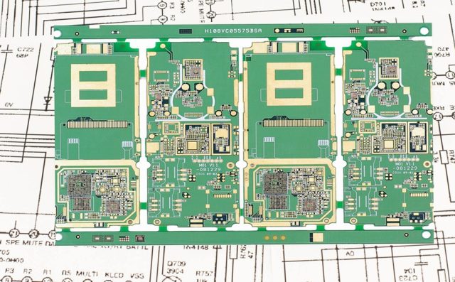
As IoT devices evolve toward higher data rates, lower power consumption, and wider connectivity, many modern IoT products now operate at high frequencies. Technologies such as 5G IoT, LPWAN, Wi-Fi 6, Bluetooth, and sub-GHz RF place strict demands on PCB performance. Developing a high frequency IoT PCB prototype is a critical step in validating RF performance, signal integrity, and system reliability before mass production.
A reliable high frequency IoT PCB prototype enables faster design iteration and reduces development risk.
What Is a High Frequency IoT PCB Prototype?

A high frequency IoT PCB prototype is a low-volume, rapid-turn PCB built specifically for RF-enabled IoT applications. These prototypes are used to verify:
-
RF signal integrity and antenna performance
-
Controlled impedance and transmission line behavior
-
Power integrity and noise isolation
-
Functional integration of RF and digital circuits
Prototyping is essential before scaling IoT designs into production.
Key Challenges in High Frequency IoT PCB Prototyping
High frequency IoT PCB prototypes face unique challenges, including:
-
Signal loss and impedance sensitivity at GHz frequencies
-
Compact board size and dense component placement
-
Mixed-signal layouts (RF + MCU + sensors)
-
Antenna matching and RF shielding requirements
Professional PCB prototyping processes are required to overcome these challenges.
Material Selection for High Frequency IoT PCB Prototypes

Material choice directly affects RF performance. Common materials for high frequency IoT PCB prototype fabrication include:
-
Rogers laminates (RO4003, RO4350)
-
Taconic RF materials
-
Low-loss FR-4 alternatives for cost-sensitive IoT designs
-
Hybrid stackups combining RF materials and FR-4
These materials offer low dielectric loss, stable Dk, and consistent RF behavior.
Impedance Control and Signal Integrity
Accurate impedance control is essential in a high frequency IoT PCB prototype, including:
-
Controlled impedance routing for RF traces
-
Precise stack-up definition and simulation
-
Tight tolerance on trace width and spacing
-
TDR impedance measurement and validation
Proper impedance control ensures reliable RF transmission and antenna efficiency.
Rapid Prototyping and Fast Turnaround
Speed is critical in IoT development. Professional high frequency IoT PCB prototype services provide:
-
Quick-turn PCB fabrication
-
Small batch prototype support
-
Fast engineering feedback and DFM review
-
Smooth transition from prototype to production
Rapid prototyping accelerates time-to-market for IoT products.
Testing and Validation for IoT PCB Prototypes
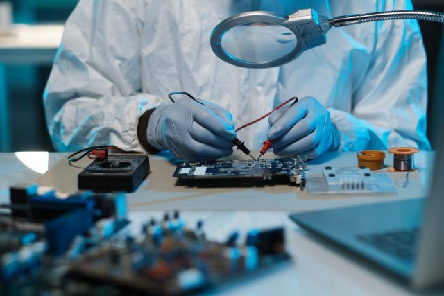
Testing ensures prototype reliability and performance, including:
-
Electrical continuity and isolation testing
-
Impedance verification
-
RF functional testing (if required)
-
Assembly inspection for prototype builds
Comprehensive validation reduces the risk of costly redesigns.
Applications of High Frequency IoT PCB Prototypes

High frequency IoT PCB prototypes are widely used in:
-
Smart home and smart city IoT devices
-
Industrial IoT (IIoT) systems
-
Wireless sensors and gateways
-
Wearable and portable IoT electronics
-
5G and RF-enabled IoT modules
These applications demand compact size and stable RF performance.
Why Choose a Professional Manufacturer for IoT PCB Prototypes?
Partnering with an experienced manufacturer for high frequency IoT PCB prototypes offers:
-
Expertise in RF and IoT PCB design support
-
Reliable material sourcing and process control
-
Fast turnaround and flexible quantities
-
Scalable path from prototype to mass production
A professional partner reduces risk and accelerates innovation.
Conclusion
A high frequency IoT PCB prototype is a crucial step in developing reliable, high-performance IoT devices. Through proper material selection, precise impedance control, rapid fabrication, and thorough testing, manufacturers can validate RF performance early and move confidently toward production.
Choosing an experienced high frequency IoT PCB prototype manufacturer ensures faster development cycles, reduced risk, and a smoother transition to scalable manufacturing.

