Control of Conductor Etching Process in Printed Circuit Boards
Copper etching is one of the most critical steps in printed circuit board (PCB) manufacturing, as it directly determines the accuracy and reliability of conductive circuit patterns. The term “printed circuit board” originates from this process, since etching is the final stage of photolithography used to define conductor geometries.
As PCB technology evolves toward higher density and finer line widths, precise control of the conductor etching process has become essential.
Role of Copper Etching in PCB Manufacturing
In PCB production, copper etching selectively removes unwanted copper from the board surface, leaving behind the designed conductive traces. This process must ensure:
-
accurate line width control,
-
minimal lateral etching (undercut),
-
consistent conductor thickness,
-
stable electrical performance.
Any deviation in etching parameters can lead to open circuits, impedance mismatch, or reduced yield.
Challenges of Fine-Line PCB Etching
Shrinking Conductor Gaps and Higher Precision Requirements
With conductor gap widths shrinking to 25–50 µm, modern HDI PCB and fine-line PCB designs place significantly higher demands on etching accuracy. Traditional etching methods often struggle with:
-
excessive sidewall dissolution,
-
uneven copper removal,
-
poor pattern replication on thick copper layers.
To address these challenges, etching technology must continuously evolve.
Advanced PCB Etching Control Technology
This study focuses on a precision conductor pattern replication technique that combines:
-
copper–ammonia etching solution composition control,
-
solution jet etching,
-
vacuum suction extraction systems.
Copper–Ammonia Etching Solution Control
A key innovation is the use of a permanent extraction device within the etching line. This system continuously removes excess dissolved copper from the etchant, maintaining a stable chemical balance between:
-
oxidized copper species,
-
active etching components.
By stabilizing the etchant composition, the etching rate remains consistent throughout the process.
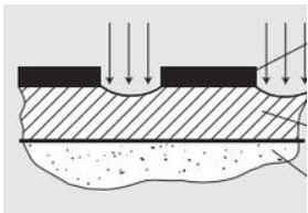
Jet Etching and Vacuum Suction for Undercut Reduction
The combined action of:
-
controlled jet stream pressure, and
-
balanced etching chemistry
ensures that copper dissolution occurs primarily at the bottom of the conductor gaps.
Key Advantages of This Approach:
-
Minimal lateral etching of conductor sidewalls
-
Near-zero dissolution in side gaps
-
Excellent pattern fidelity even with thick copper foils or plated layers
-
Improved control of conductor geometry
This results in highly accurate fine-line circuits suitable for advanced PCB applications.
Environmental Benefits of Controlled Etching Processes
Beyond technical performance, this etching control technology also improves environmental sustainability in industrial PCB production:
-
Reduced chemical waste
-
More efficient copper removal and recovery
-
Lower overall etchant consumption
These advantages align with the growing demand for greener PCB manufacturing processes.
Etching Chemistry and Oxidation Mechanisms
In PCB manufacturing, various etch resists and selective metal etching techniques have been tested over the years. Despite differences in materials and formulations, all copper etching processes share a common principle:Copper etching relies on the oxidation of metallic copper followed by the dissolution of the resulting copper oxides or complexes.
Understanding and controlling this oxidation–dissolution mechanism is fundamental to achieving stable, high-precision etching results.
As PCB designs continue to move toward finer lines and higher densities, precise control of the conductor etching process is no longer optional—it is essential. Advanced copper–ammonia etching systems combined with jet etching and vacuum extraction offer:
-
superior fine-line pattern accuracy,
-
reduced undercutting,
-
stable process control,
-
improved environmental performance.
These technologies represent an important step forward in high-density PCB manufacturing and next-generation circuit pattern formation.
