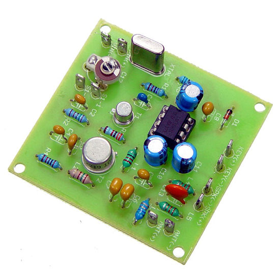
Modern wireless systems—from satellite communication payloads to 5G/6G infrastructure and defense-grade radar—depend on the precision, stability, and reliability of RF Transceiver PCB architectures. As operating frequencies rise into the sub-6 GHz, Ku-, Ka-, and mmWave bands, the RF Transceiver PCB becomes the defining foundation for signal integrity, phase coherence, and power efficiency. High-frequency electronics demand PCB structures that minimize loss, control impedance, suppress interference, and maintain stable electrical behavior across extreme environments.
A well-engineered RF Transceiver PCB directly affects the performance of LNAs, PAs, mixers, LO chains, beamforming ICs, synthesizers, and RF switches—components whose function depends on predictable transmission and clean electromagnetic behavior. Below is a deep technical examination of how material science, stackup planning, and RF layout engineering collectively shape next-generation RF Transceiver PCB performance.
1. Material Engineering for Low-Loss and Phase-Stable RF Transceiver PCB Platforms
The electrical behavior of an RF Transceiver PCB is governed by the dielectric constant (Dk), dissipation factor (Df), and conductor roughness of the selected laminate. To maintain phase stability and low insertion loss across high-frequency bands, RF engineers must select:
Low-Dk materials for predictable impedance
Ultra-low Df laminates to reduce dielectric loss
Smooth-foil copper to minimize conductor loss at mmWave
Temperature-stable dielectric formulations for orbital or outdoor operation
High-performance materials such as PTFE composites, hydrocarbon ceramics, and modified epoxy systems enable RF Transceiver PCB structures to deliver consistent propagation velocity, minimal phase drift, and wideband signal transparency.
2. Multi-Layer RF Transceiver PCB Stackups for High-Bandwidth Signal Chains
RF transceivers require tightly controlled stackups that manage both microwave routing and digital control paths. High-frequency routing typically uses:
Stripline structures for isolation-sensitive LO or IF paths
Microstrip layers for wideband antenna feed networks
Hybrid dielectric stackups for RF–digital co-integration
Back-drilled vias to suppress via stubs at high frequencies
These stackup techniques ensure that RF Transceiver PCB high-speed paths maintain constant impedance and minimize signal reflection, a critical requirement for phased-array and multi-band transceiver modules.
3. High-Density Interconnect (HDI) Layout to Optimize RF Transceiver PCB Compactness
As RF modules shrink in size, RF Transceiver PCB designs must incorporate HDI technologies, including:
Laser-drilled microvias for RFIC breakout
Via-in-pad structures to reduce inductive parasitics
Embedded passives for filter, matching, and bias networks
Stacked microvias for vertical RF transitions with minimal loss
These advanced interconnect solutions allow the RF Transceiver PCB to support compact, high-density routing without degrading high-frequency performance.
4. Electromagnetic Control and Crosstalk Mitigation in RF Transceiver PCB Routing
Given the coexistence of power amplifiers, LNAs, oscillators, and digital processors, electromagnetic isolation is a defining challenge in RF Transceiver PCB development. Engineers use:
Ground fences and via stitching
Dedicated RF shields and cavity structures
Controlled reference planes for stable return paths
EM-simulated transitions to eliminate discontinuities
These measures preserve signal purity across dense RF blocks, critical for multi-channel transceiver arrays and satellite communication chains.
5. Thermal and Mechanical Reliability of RF Transceiver PCB Systems
High-power RF outputs generate thermal stress that may degrade performance or destabilize phase alignment. A robust RF Transceiver PCB must incorporate:
Thermal-via arrays for vertical heat transfer
Copper balancing to prevent warpage
CTE-matched laminates for aerospace use
Low-outgassing materials for space payloads
These structural choices ensure that RF Transceiver PCB platforms maintain stable performance over extreme temperature cycles and long mission durations.
6. The Central Role of RF Transceiver PCB Technology in Future Communication Systems
The move toward multi-band operation, scalable phased arrays, and compact RF front ends places unprecedented demands on RF Transceiver PCB engineering. Whether for satellite payloads, 5G/6G macro cells, UAV communication modules, or high-performance radar, the RF Transceiver PCB remains the keystone that binds RF system performance, reliability, and integration density.
As frequency bands expand and power levels rise, next-generation RF systems will increasingly rely on innovations in RF Transceiver PCB stackups, material science, and EM-driven layout optimization.
