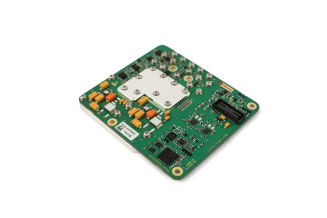
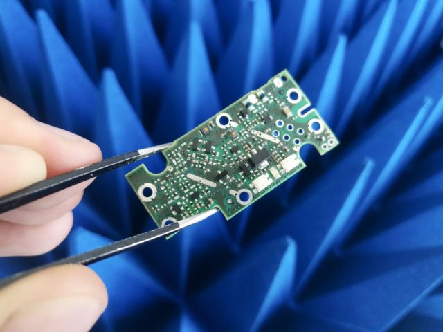
Next-generation RF transceivers—whether for 5G mmWave, SATCOM terminals, phased-array antennas, or short-range high-bandwidth links—place brutal demands on PCB materials. To maintain ultra-low insertion loss, wideband consistency, stable phase response, and clean radiation efficiency, mmWave module PCB materials must deliver precision alignment, ultra-low dielectric loss, tight Dk control, and minimal copper roughness across every layer.
In mmWave bands above 24 GHz, even microscopic deviations become performance killers. Small misalignments in the PCB stack-up distort RF pathways; fluctuations in dielectric constant break phase matching; excess copper roughness raises insertion loss; thermal drift changes impedance. This is exactly why high-frequency engineers rely on precision-aligned mmWave module PCB materials: engineered laminates that keep RF transceivers stable across ultra-wide bandwidths.
Why Precision-Aligned mmWave PCB Materials Matter
High-frequency PCB materials directly control signal loss, impedance accuracy, and RF stability. For mmWave modules, the stakes are higher. Signals are short-wavelength, high-energy, and hypersensitive to any structural or dielectric imperfection. To deliver reliable wideband consistency, materials must keep insertion loss low while preserving the phase structure of the RF waveform.
Materials such as ultra-low-loss PTFE composites, ceramic-filled hydrocarbon laminates, and next-gen low-roughness copper foils provide the dimensional and electrical stability mmWave engineers depend on. With Df values below 0.002, these laminates significantly reduce insertion loss at 28 GHz, 39 GHz, and even above 60 GHz, allowing RF transceivers to maintain cleaner EVM and higher modulation orders.
Ultra-Low Insertion Loss: The Core Metric
Insertion loss dominates mmWave system design. Every connector, trace, dielectric layer, and copper interface contributes to attenuation. High-performance PCB materials use chemically treated low-roughness copper and stable dielectric structures to keep losses minimal. This allows RF transceivers to maintain output power, avoid noise-floor collapse, and support wideband signals without distortion.
With ultra-low insertion loss PCB materials, mmWave modules show stronger link budgets, longer ranges, cleaner constellation diagrams, and better overall RF performance in 5G, automotive radar, and SATCOM systems.
Wideband Consistency from 24 GHz to 70 GHz
Wideband consistency defines whether an RF transceiver can hold stable performance across broad frequency ranges. Materials with tightly controlled dielectric constant (Dk) ensure predictable propagation velocity, accurate phase matching, and stable filter performance. When Dk varies, wideband systems lose calibration, steering errors grow, and antenna array gain collapses.
Precision-aligned mmWave PCB laminates solve this with:
-
extremely uniform Dk across sheets,
-
low thermal drift,
-
stable mechanical properties,
-
minimal moisture absorption (critical above 40 GHz).
These characteristics let next-gen RF modules maintain consistent impedance, predictable phase delay, and uniform performance across multi-GHz-wide operating bands.
Enabling Next-Gen RF Transceiver Architecture
RF transceivers evolving toward higher bandwidth and tighter beamforming require PCB materials capable of:
-
maintaining ultra-low insertion loss even in dense multilayer mmWave modules,
-
supporting hybrid RF/digital architectures with stable dielectric performance,
-
preserving signal integrity under thermal stress and power cycling,
-
enabling ultra-precise alignment for high-density BGA, flip-chip, and antenna-in-package (AiP) designs.
These capabilities define the future of 5G mmWave radios, FR2 base stations, phased arrays, automotive radar modules, and 6G-class RF front-ends.
The Material Foundation for the 6G Era
As systems move toward 100 GHz and above, PCB materials will be the first battlefield. Ultra-low-loss laminates, precision-aligned dielectric stacks, and advanced thin-copper foils will determine whether next-gen RF transceivers can keep pace. Engineers using these materials gain cleaner signal paths, reduced power consumption, and higher reliability in harsh environments—laying the groundwork for 6G, massive-MIMO evolution, and sub-THz sensing.
These PCB materials are not simply substrates—they are the electromagnetic scaffolding on which the entire RF future stands.
