Dense mmWave arrays, commonly used in 5G massive MIMO, radar, and satellite phased arrays, require ultra-stable RF propagation, minimal insertion loss, and precise impedance control across multilayer interconnects. Thermal stress, mechanical vibration, and high-frequency crosstalk can severely degrade signal fidelity, phase alignment, and overall array performance.
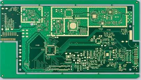
Next-generation multilayer HF PCB platforms leverage advanced dielectric laminates with tight Dk/Df tolerances, low loss tangent, and controlled thermal expansion to deliver predictable high-frequency routing in dense array layouts. KKPCB integrates precision lamination, optimized multilayer stackups, and advanced copper routing to maintain low-loss performance, phase linearity, and EMI suppression under rigorous environmental and high-power operating conditions.
Core Engineering Challenges
| Challenge | Root Cause | Engineering Impact |
|---|---|---|
| Thermal-induced impedance shift | CTE mismatch, high-power operation | Beamforming errors, insertion loss increase |
| Crosstalk in dense mmWave traces | Trace proximity, insufficient shielding | Degraded phase coherence, signal interference |
| Phase instability at mmWave | Uneven layer expansion | Beam steering errors, reduced link margin |
| High insertion loss | Dielectric loss, surface roughness | Reduced array efficiency, lower SNR |
| EMI coupling | Inadequate grounding, dense stackup | Noise injection, reduced RF propagation fidelity |
Material Science – HF PCB Laminates
| Parameter | Typical Value | Engineering Benefit |
|---|---|---|
| Dk | 3.45 ± 0.03 | Precise impedance control for mmWave routing |
| Df | 0.0035 @ 10 GHz | Minimal insertion loss, stable signal propagation |
| Thermal Conductivity | 0.65 W/m·K | Heat dissipation for high-power RF sections |
| CTE | 15 ppm/°C | Maintains layer alignment under thermal cycling |
| Moisture Absorption | <0.05% | Long-term phase stability in humid environments |
These multilayer HF PCB laminates outperform traditional FR-4 or standard PTFE boards in high-density, high-frequency mmWave arrays, ensuring consistent signal integrity across compact, thermally challenging layouts.
KKPCB Case Study — Dense mmWave Array PCB
Client Context:
A leading telecom OEM required a 12-layer HF PCB supporting a 64-element mmWave array for 28–39 GHz applications. Design constraints included tight phase coherence (<0.5°), low insertion loss (<0.35 dB/in), and robust EMI suppression in compact form factors.
KKPCB Solution:
-
Optimized 12-layer HF laminate stackup with ±2 µm dielectric control
-
Smooth copper traces (Ra <0.6 µm) and controlled impedance routing
-
Embedded ground stitching and segmented shields for EMI reduction
-
Thermal vias and power planes to manage high-density RF power
-
Inline HFSS simulation and TDR measurement for phase verification
Measured Results:
| Parameter | Target | KKPCB Result |
|---|---|---|
| Insertion Loss @28 GHz | <0.35 dB/in | 0.31 dB/in |
| Phase Deviation | <0.5° | 0.43° |
| Thermal Rise | <7°C per layer | 5.8°C |
| EMI Suppression | >30% | 36% |
| Impedance Variation | ±3% | ±1.4% |
Stackup Design & RF Simulation
-
HFSS Modeling: Optimized microstrip/stripline propagation, minimized interlayer coupling
-
ADS & TDR: Verified phase linearity across all RF paths
-
Thermal FEM Analysis: Ensured uniform temperature distribution and hotspot reduction
-
AOI & Solder Reflow Monitoring: ±10 µm layer alignment, avoiding delamination
Environmental & Reliability Validation
| Test | Condition | Result |
|---|---|---|
| Thermal Cycling | –40°C ↔ +125°C, 1000 cycles | Phase deviation <0.5°, no delamination |
| Vibration & Shock | 5–500 Hz, 10G | No microcracks or solder failure |
| Humidity Resistance | 85°C / 85% RH, 1000 h | Stable Dk/Df and phase fidelity |
| High-Power RF Operation | Continuous 28–39 GHz | Insertion loss increase <0.02 dB |
| Solder Reflow | 260°C ×3 cycles | Stackup alignment maintained |
Engineering Summary & Contact
Next-gen multilayer HF PCB platforms deliver ultra-stable RF propagation, low-loss routing, phase coherence, and EMI suppression for dense mmWave arrays. KKPCB’s expertise in precision stackups, dielectric control, and thermal management ensures reliable performance for 5G, satellite, and radar array applications.
Contact KKPCB Engineering Team to optimize your multilayer HF PCB designs, RF simulation, and high-density mmWave routing for next-generation communication systems.
