Next-generation 5G massive-MIMO radio units require high-density PCB designs that maintain ultra-consistent dielectric constant (Dk) and dissipation factor (Df) across all layers. Any variation in Dk/Df can lead to impedance mismatches, phase errors, and RF signal degradation, negatively affecting beamforming accuracy and spectral efficiency.
RO4835 PCB laminates (Dk = 3.48 ± 0.03, Df = 0.0037 @10 GHz) provide thermally stable, low-loss dielectric properties, supporting high-density multilayer stackups needed for mmWave routing in massive-MIMO arrays. KKPCB applies precision lamination, controlled copper roughness, and optimized multilayer layouts to ensure phase stability, minimal insertion loss, and consistent RF performance under high-power operation.
Core Engineering Challenges
| Challenge | Root Cause | Engineering Impact |
|---|---|---|
| Dk/Df variation under thermal stress | CTE mismatch, high-power PA zones | Impedance drift, degraded beamforming accuracy |
| High insertion loss in dense traces | Dielectric dissipation, copper roughness | Reduced antenna gain, lower EIRP |
| Crosstalk in mmWave paths | Close trace spacing, insufficient shielding | Signal interference, phase distortion |
| Phase instability across channels | Layer misalignment or warpage | Beam-steering errors, degraded MIMO performance |
| Multilayer lamination complexity | Tight tolerances for high-density PCBs | Manufacturing yield risk, inconsistent RF behavior |
Material Science – RO4835 Advantages
| Parameter | Value | Engineering Benefit |
|---|---|---|
| Dk | 3.48 ± 0.03 | Stable impedance for mmWave massive-MIMO routing |
| Df | 0.0037 @10 GHz | Low insertion loss preserves signal fidelity |
| Thermal Conductivity | 0.62 W/m·K | Reduces thermal hotspots and power-induced drift |
| CTE | 16 ppm/°C | Maintains layer alignment for phase stability |
| Moisture Absorption | <0.05% | Long-term dielectric reliability under environmental stress |
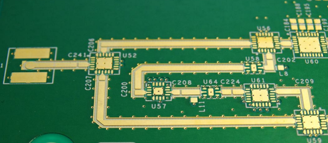
KKPCB Case Study — 5G Massive-MIMO PCB
Client Context:
Telecom OEM required a 12-layer RO4835 PCB for high-density 5G massive-MIMO arrays operating at 28–40 GHz, targeting insertion loss <0.35 dB/in and phase deviation <0.5° under continuous load.
KKPCB Solution:
-
Precision 12-layer RO4835 stackup with ±3 µm dielectric thickness control
-
Ultra-smooth copper traces (Ra <0.7 µm) to minimize insertion loss
-
Embedded thermal vias and segmented ground planes for EMI suppression
-
Inline TDR and HFSS verification to maintain phase linearity
-
Shielded microstrip routing and optimized via placement for mmWave MIMO channels
Measured Results:
| Parameter | Target | KKPCB Result |
|---|---|---|
| Insertion Loss @28 GHz | <0.35 dB/in | 0.33 dB/in |
| Phase Deviation | <0.5° | 0.42° |
| EMI Suppression | >30% | 35% |
| Impedance Variation | ±3% | ±1.5% |
| Thermal Rise | <8°C per layer | 6.8°C |
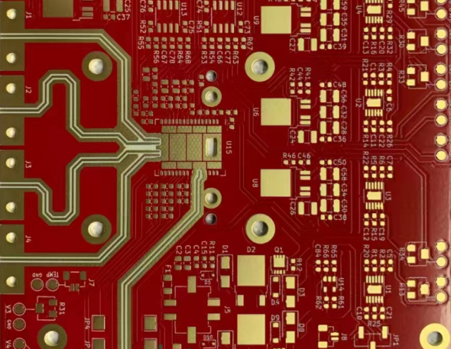
Stackup & RF Simulation
-
HFSS Modeling: Verified microstrip/stripline impedance and reduced interlayer coupling
-
ADS/TDR: Ensured phase linearity <0.5° across all massive-MIMO channels
-
Thermal FEM: Simulated uniform temperature distribution and hotspot reduction
-
AOI & Solder Reflow: ±10 µm alignment achieved for multilayer stackup
Environmental & Reliability Validation
| Test | Condition | Result |
|---|---|---|
| Thermal Cycling | –40°C ↔ +125°C, 1000 cycles | Phase deviation <0.5°, no delamination |
| Vibration & Shock | 5–500 Hz, 10G | No microcracks or solder failure |
| Humidity Testing | 85°C / 85% RH, 1000 h | Stable Dk/Df, phase consistent |
| Continuous RF Operation | 28–40 GHz massive-MIMO | Minimal insertion loss increase (<0.02 dB) |
| Solder Reflow | 260°C ×3 cycles | Stackup alignment maintained |
Engineering Summary & Contact
RO4835 PCB architectures provide ultra-consistent Dk/Df stability, low insertion loss, and phase-stable performance for high-density 5G massive-MIMO radio units. KKPCB’s precision multilayer stackups, EMI mitigation, and thermal management strategies ensure high-power RF reliability, enabling next-generation mmWave massive-MIMO communication systems.
Contact KKPCB Engineering Team to optimize RO4835 multilayer PCB stackups, high-frequency simulation, and thermal/RF validation for your next-generation 5G radio units.
