Aerospace navigation and telemetry links depend on signals that simply cannot drift, distort, or wander off-phase. Whether guiding a launch vehicle or stabilizing a satellite’s inter-orbital communication, the RF path must maintain tight impedance control, predictable phase behavior, and ultra-low distortion across multi-GHz carriers. This is where Impedance Controlled PCB architectures become fundamental—not an optional design luxury, but the backbone of reliable aerospace communication.
Impedance Control: The Stabilizing Spine of Wideband RF Chains
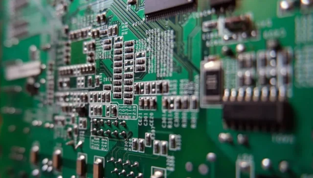
In aerospace modules, RF amplifiers, mixers, PLLs, filters, and telemetry transceivers all demand interconnects that present a uniform transmission environment. Any deviation from the target 50 Ω or 100 Ω differential impedance—even ±5%—can trigger standing waves, coupling spikes, amplitude ripple, and unwanted group-delay variations.
Advanced Impedance Controlled PCB stackups mitigate these pitfalls by aligning dielectric properties, copper roughness, trace geometry, and ground-reference stability to maintain consistent impedance across temperature extremes, vibration loads, and long-duration orbital exposure.
Fiberglass-reinforced low-Dk materials, ceramic-filled laminates, and PTFE composites allow designers to hit impedance targets with high repeatability, even when dealing with multi-layer routing in compact aerospace form factors.
Driving RF Linearity Through Low-Loss and Predictable Transmission Paths
RF linearity—how faithfully a system preserves the shape of a signal—depends heavily on the linearity of the interconnect medium itself.
If the PCB introduces dielectric absorption, impedance mismatch, or micro-scale resonances, front-end components must compensate through extra gain or filtering, creating a chain reaction of distortion.
Impedance Controlled PCB engineering improves RF linearity by:
• Minimizing insertion loss at high frequencies through smooth copper and low-loss dielectrics
• Keeping the effective propagation constant uniform across layers
• Preventing intermodulation products arising from discontinuities in transmission paths
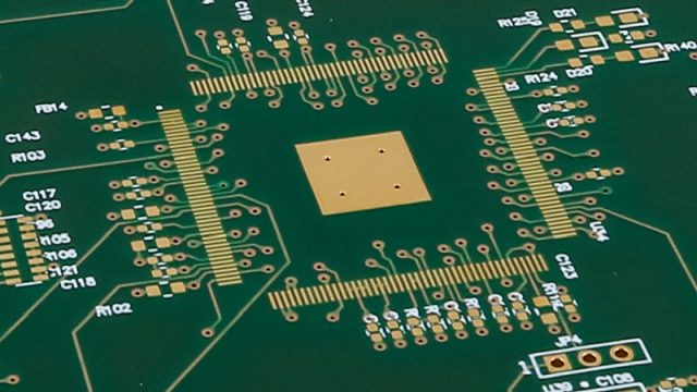
• Ensuring PCB vias, blind vias, and launch pads exhibit controlled transition impedance
The result is a transmission network where the PCB does not contaminate the signal, allowing high-linearity LNAs, PAs, and mixers to perform near their theoretical limits.
Phase Consistency: Critical for Navigation Accuracy and Telemetry Lock
Aerospace telemetry and navigation signals rely on coherent phase relationships that enable Doppler measurement, pseudorange calculations, and closed-loop control. Phase drift—even fractions of a degree—can degrade positioning accuracy and destabilize feedback systems.
Impedance Controlled PCB architectures strengthen phase consistency through:
• Stable Dk/Df values that do not fluctuate with operational temperature cycles
• Cone-controlled microstrip and stripline geometries with uniform dielectric loading
• Tight interlayer registration eliminating asymmetry in differential routing
• Precision-engineered reference planes suppressing modal conversion
When the phase velocity remains constant, the system can sustain lock-tight synchronization even under aerospace-grade thermal shock, altitude variations, and long-duration electromagnetic exposure.
Aerospace-Ready Reliability Through High-Frequency Discipline
Navigation and telemetry modules operate in harsh environments where mechanical stress, cosmic radiation, rapid pressurization changes, and aggressive thermal cycles are daily realities.
Impedance Controlled PCB designs support aerospace reliability by applying:
• Low-thermal-drift substrates to maintain RF stability across –55 °C to +150 °C
• Layer-balanced stackups preventing warpage and impedance migration
• Via-field optimization reducing parasitic inductance and suppressing EMI pathways
• Shielding-oriented routing protecting delicate RF channels from platform-generated noise
The combination of mechanical stability and electromagnetic discipline creates a PCB platform that behaves predictably for years, not just hours.
Conclusion
Aerospace navigation and telemetry modules cannot tolerate RF uncertainty. The path between components must behave as mathematically as the waveforms they carry. By integrating Impedance Controlled PCB architectures, engineers unlock a level of RF linearity, phase consistency, and wideband reliability that directly translates to safer launches, more stable spacecraft, and more dependable telemetry links.
