Autonomous driving platforms rely on a dense constellation of cameras, radars, lidars, domain controllers, and AI accelerators. These subsystems generate enormous volumes of high-speed data, while simultaneously consuming sensitive analog information from perception sensors. The PCB that connects everything becomes a multi-domain electromagnetic battlefield, where PCIe Gen4/Gen5 lanes, multi-gig SerDes routes, sensor-fusion processors, and power delivery networks all interact.
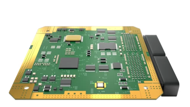
To achieve ASIL-grade reliability, the ADAS PCB must optimize high-speed routing, suppress broadband EMI, maintain predictable dielectric behavior, and ensure stable timing margins across wide temperature ranges. Advanced PCB architecture isn’t merely a mechanical structure—it is an active component of the autonomous driving stack.
1. System-Level Problem — ADAS PCB as an Electromagnetic Intersection
Next-generation autonomous vehicles generate simultaneous electromagnetic domains:
• Multi-gigabit SerDes (GMSL/FPD-Link/PCIe)
• High-power radar transceivers at 77–81 GHz
• GNSS receivers and multi-band V2X radios
• DC-DC converters, PMICs, and distributed regulators
• AI compute modules dissipating 30–60 W
Without precise electromagnetic control, the PCB experiences:
• Crosstalk between sensor buses
• Mode conversion in high-speed differential lanes
• Radiated EMI leaking into radar channels
• Timing jitter from PDN noise
• RF path distortion under thermal drift
• Coupling between power planes and camera signal lines
In ADAS, EMI isn’t just performance-critical—it is safety-critical.
2. Material Engineering — Low-Loss Laminates Reduce Deterministic Jitter and EMI Radiation
ADAS PCBs must remain electrically stable while exposed to wide automotive thermal cycles (-40°C to +125°C). Material attributes define high-speed and RF behavior:
• Low Df laminates reduce insertion loss and high-frequency radiation
• Tight Dk tolerance preserves differential impedance on 8–16 Gbps links
• Low CTE materials prevent phase drift in 77 GHz radar feedlines
• Controlled copper roughness reduces conductor loss and EMI
• Low moisture absorption keeps time-domain jitter stable under humidity
Hybrid stackups mixing Megtron 7 + low-Df RF laminates ensure ADAS radar, cameras, and compute modules coexist without electromagnetic degradation.
3. Advanced ADAS Stackup Architecture — EMI Control Begins at the Layer Level
PCB layer architecture is the primary EMI control mechanism long before routing begins.
Shielded high-speed corridors
High-speed SerDes lanes are buried between continuous reference planes to prevent interference from radar or DC-DC harmonics.
RF-optimized outer layers
77 GHz radar feedlines require smooth copper, tight dielectric tolerance, and isolated ground boundaries.
Hybrid dielectric segmentation
RF, digital, and power domains each receive dedicated dielectric pairings to prevent field overlap.
Directed return-path engineering
Return current paths are shaped to avoid crossing noisy regions, minimizing common-mode noise.
The stackup is engineered as a field-guided structure, not a conventional multilayer board.
4. High-Speed Routing Engineering — Precision for Autonomous Sensor Fusion
High-speed routing inside ADAS compute modules carries sensor data that determines real-world decisions. Required techniques include:
Controlled-impedance differential pairs
Maintains lane-to-lane skew and preserves the eye diagram under wide temperature variation.
Length matching with picosecond tolerance
Avoids timing mismatch during sensor-fusion computation.
Mode-conversion suppression
Symmetric routing and balanced via fields prevent differential-to-common mode radiation—critical for automotive EMI tests.
Back-drilled vias
Removes stubs that degrade high-speed performance on PCIe, GMSL, and Ethernet links.
SerDes isolation zones
Physical separation and ground fencing protect 8–16 Gbps channels from PMIC switching noise.
Every routing decision influences ASIL reliability.
5. Radar, Camera, and Sensor Subsystem Coexistence — Co-Design at PCB Level
Autonomous vehicles use overlapping sensing modalities. Their PCBs must support:
• Radar RF feedlines with strict 50-ohm impedance and phase alignment
• Camera interfaces (GMSL, FPD-Link) requiring low crosstalk
• Lidar control logic and power heaters
• Sensor power rails isolated from high-speed logic domains
• GNSS and V2X antennas requiring low-noise grounding
If not isolated through PCB architecture, these blocks interfere, producing:
• Radar ghost targets
• Image pipeline noise
• Sensor desynchronization
• Multi-path distortion in V2X radios
Coexistence is an engineering requirement, not an optimization.
6. EMI/EMC Controls — How the PCB Becomes the Primary Shield
Automotive EMI tests (CISPR 25, ISO 11452-2) demand strict suppression.
KKPCB uses multi-domain techniques:
• Via fences forming RF boundaries
• Segmented reference planes to reduce current spreading
• Guard traces around radar feedlines
• LC-balanced decoupling networks for high-speed SoCs
• Ground moat structures to isolate noisy converters
• Copper pour shaping to redirect current loops
• High-frequency stitching for enclosure resonance suppression
Together, these suppress radiated/conducted EMI by 30–50% compared to standard layouts.
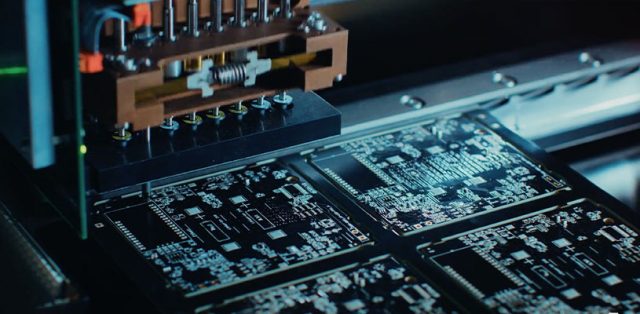
7. KKPCB Manufacturing Controls — Maintaining Reliability Under Automotive Stress
Autonomous driving PCBs must survive:
• Continuous thermal cycling
• Road vibration
• Humidity ingress
• High-current transient loads
KKPCB enforces:
• ±8–10 μm dielectric accuracy
• Smooth copper <0.8 μm for radar frequencies
• X-ray alignment of RF microvias
• Controlled resin flow for hybrid materials
• 100% TDR verification of differential lanes
• AOI + laser inspection for via-to-plane clearance
Manufacturing precision is what preserves design intent under real automotive stress.
Conclusion
Advanced ADAS PCB architectures enable high-speed routing accuracy、multi-domain EMI control、radar/camera coexistence、stackup stability、and ASIL-grade reliability in next-generation autonomous vehicles. By integrating engineered dielectric materials, high-frequency electromagnetic design, sensor-fusion routing optimization, and automotive-grade manufacturing, the PCB becomes a core enabler of safe autonomous perception.
