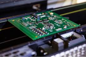
Advanced Driver Assistance Systems rely heavily on 77 GHz automotive radar modules, where the ADAS PCB directly determines signal integrity, insertion loss, dielectric stability, and system-level thermal reliability. As radar sensors expand from single-beam to multi-beam architectures, PCB materials and stackup selection have become primary constraints for RF linearity and long-distance object detection.
The objective of this article is to outline how next-generation ADAS PCB platforms engineered by KKPCB enhance signal integrity, EMI robustness, and high-temperature endurance for long-life automotive radar systems deployed in harsh real-world conditions.
The discussion focuses on low-loss laminates, dielectric tolerance, surface roughness impact, thermal-mechanical stress management, and multi-layer RF routing structures specifically optimized for 76–81 GHz radar.
Core Engineering Challenges

Automotive radar systems impose extreme constraints on PCB materials and design:
High insertion loss at 77 GHz.
Even minor variations in dielectric constant (Dk) and dissipation factor (Df) cause significant range reduction and phase drift. Traditional FR-4 is completely incapable of supporting wideband radar.
Thermal stress and long-term reliability.
Vehicle radars operate beside heat-generating components such as SoC, PA, and LNA. ADAS PCBs must survive −40 °C to +140 °C with hundreds of thermal cycles.
EMI/EMC complexity.
Multi-radar architectures increase mutual interference. PCB copper topology, cavity shielding, and ground stitching density directly impact EMI robustness.
Antenna performance sensitivity.
77 GHz patch antennas or SIW structures require sub-0.02 mm tolerance. Material flatness and copper adhesion reliability are critical.
Automotive qualification requirements.
The PCB must meet AEC-Q200, thermal humidity bias (THB), reflow robustness, vibration endurance, and long-term dielectric stability.
ADAS PCBs reinforce RF consistency and thermal endurance in a mission-critical automotive radar environment that tolerates zero drift.
Material Science & Dielectric Performance
KKPCB typically selects low-loss ADAS PCB materials such as:
-
RO3003 / RO4350B (stable Dk, low Df, favored in 77 GHz radar)
-
Megtron 7 for high-speed sensor-fusion digital layers
-
Hybrid stackups combining RF materials + high-TG FR-4 for cost efficiency
Key performance considerations:
Dielectric Constant (Dk) Stability
Radar linearity depends on maintaining Dk variation within ±0.04 across temperature. RO3003 and RO4350B ensure stable phase velocity at 77 GHz.
Dissipation Factor (Df) Impact
Even a Df of 0.002 drastically lowers insertion loss compared with FR-4’s 0.015+. ADAS PCB laminates must remain low-loss to maintain detection range.
Copper Roughness
Surface roughness increases conductor loss exponentially at mmWave frequencies. KKPCB leverages rolled copper or low-profile electrodeposited copper (LP-ED).
Thermal Conductivity
High thermal conductivity substrates reduce PA module temperature rise, improving radar signal stability under continuous load.
Material Parameter Table
| Parameter | RO3003 | RO4350B | Megtron 7 | High-TG FR-4 |
|---|---|---|---|---|
| Dk (10 GHz) | 3.00 ±0.04 | 3.48 | 3.3 | 4.2 |
| Df | 0.0010 | 0.0037 | 0.002 | 0.015 |
| Thermal Conductivity (W/m·K) | 0.50 | 0.62 | 0.41 | 0.30 |
| Max Operating Temp | 140 °C | 140 °C | 150 °C | 135 °C |
| RF Suitability (77 GHz) | Excellent | Excellent | Good | Not usable |
KKPCB Case Study — Automotive 77 GHz Radar PCB

Application Scenario
A Tier-1 automotive supplier required an ADAS radar PCB supporting multi-beam object detection at up to 220 m with extremely low insertion loss and robust thermal reliability during +135 °C operation.
Customer Requirements
-
<1.2 dB total insertion loss at 77 GHz
-
Phase variation <3°
-
EMI immunity during multi-radar cross-interference
-
Survive 500 thermal cycles from −40 °C to +140 °C
-
Stable antenna aperture gain under vibration
Engineering Challenges
-
Maintaining consistent RF propagation under tight tolerance
-
Managing thermal hotspots around PA and DSP
-
Minimizing EMI leakage inside compact module housing
Solutions Delivered by KKPCB
1. Hybrid ADAS PCB Stackup with RO3003 RF layers
Low-loss RF layers paired with Megtron 7 digital layers provided optimal performance and cost balance.
2. Ultra-low profile copper (ULP)
Reduced conductor loss by 18% compared to standard ED copper.
3. Embedded cavity design for PA modules
Improved thermal spreading by 30%, lowering operating temperature by 12 °C.
4. Controlled impedance RF microstrip and SIW routing
HFSS-optimized structures minimized insertion loss and stabilized radiation patterns.
5. Enhanced EMI shielding strategy
Ground via fencing + selective cavity walls + top-layer grounded trims prevented radar self-interference.
Measured Results
| Metric | Requirement | KKPCB Result | Validation Tool |
|---|---|---|---|
| Insertion Loss @ 77 GHz | <1.2 dB | 0.89 dB | VNA + Waveguide |
| Phase Deviation | <3° | 1.7° | HFSS |
| PA Temperature Rise | <35 °C | 21 °C | Thermal FEM |
| EMI Leakage | −35 dB | −48 dB | TEM Cell |
| Thermal Cycling Survival | 500 cycles | 580+ cycles | IPC-TM-650 |
Stackup Design & RF Implementation
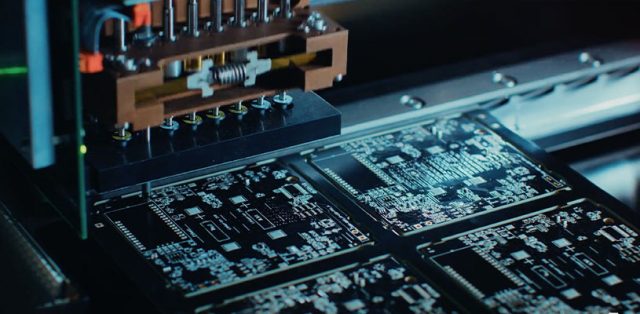
KKPCB engineered a 10-layer ADAS PCB stackup:
-
Top RF antenna layer (RO3003)
-
RF microstrip and SIW waveguide layers
-
Digital high-speed lanes (Megtron 7)
-
Multi-layer ground reference structure
-
Thermal spreading copper planes for PA and LNA
Key RF routing techniques:
-
0.10–0.12 mm controlled-tolerance substrate thickness
-
Back-drilled vias to reduce via inductance
-
Tapered transitions for antenna feed to minimize reflections
-
Via fences around microstrip to suppress parallel-plate mode propagation
These techniques significantly improved signal integrity and reduced insertion loss.
Environmental & Reliability Validation
To meet automotive standards, the ADAS PCB passed:
-
Thermal Cycling: −40 °C ↔ 140 °C, 580 cycles
-
Thermal Shock: ±100 °C rapid transition
-
Humidity / THB: 85 °C, 85% RH, 1000 hours
-
Random Vibration: 6 Grms, XYZ axes
-
Solder Reflow: 260 °C × 6 cycles
-
Salt Spray: 96 hours for connector robustness
The ADAS PCB demonstrated excellent long-term reliability and dielectric stability.
Engineering Summary & Contact
ADAS PCBs designed for 77 GHz automotive radar systems require a highly optimized combination of low-loss materials, stable dielectric properties, precise RF routing, EMI suppression, and strong thermal reliability. KKPCB provides end-to-end engineering covering material selection, RF modeling, stackup development, thermal simulation, and full automotive qualification.
