The Importance of Via Placement in PCB Design
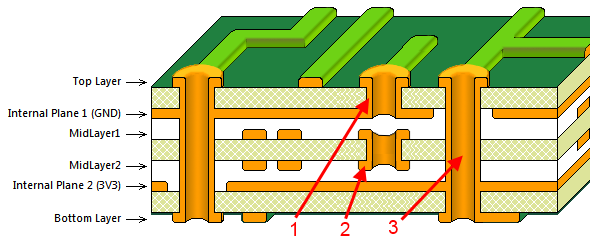
In PCB design, via positioning plays a crucial role in ensuring electrical performance, manufacturing reliability, and signal integrity. Improper via placement—especially placing vias directly on component pads—can lead to soldering defects, electrical noise, and higher production costs.
This article explains why vias should be staggered from pad positions, the engineering logic behind it, and practical tips to achieve an optimized PCB layout.
1. Preventing Solder Loss and Ensuring Solder Quality
Pad and Via Functionality
Pads are essential interfaces connecting component leads to PCB copper traces. Reliable solder joints depend on sufficient solder volume and consistent heat distribution.
When vias are placed directly on pads, molten solder can flow through via holes, leaking to the other side of the board. This causes:
-
Insufficient solder on the pad
-
Cold solder joints or voids
-
Reduced mechanical strength
Design Solution
By staggering via positions away from pads, solder remains on the pad surface, forming a stable and durable joint. This simple adjustment significantly improves soldering yield and connection reliability.

2. Avoiding Signal Interference and Enhancing Signal Integrity
High-Speed Signal Sensitivity
For high-frequency or high-speed PCB designs, vias located directly on pads can create parasitic capacitance and inductance, resulting in:
-
Signal reflections
-
Crosstalk between adjacent traces
-
Impedance mismatches
Best Practice
Move vias slightly off the pad area and, where necessary, apply back-drilling or blind/buried via techniques to reduce unwanted parasitic effects. This helps maintain clean impedance control and signal quality across differential pairs.
3. Reducing Manufacturing Costs and Improving Yield
Manufacturing Risks of Vias on Pads
During the PCB drilling process, small drill deviations can damage the pad copper, increasing the scrap rate. Additionally, via plugging (used to prevent solder leakage) complicates production and increases cost.
Practical Optimization
-
Keep vias staggered from pads
-
Group vias in dedicated zones for better control
-
Avoid unnecessary via plugging
This approach simplifies production and enhances Design for Manufacturability (DFM).
4. Optimizing Thermal Management and Preventing Overheating
The Role of Thermal Vias
For power components and heat-sensitive devices, good thermal management is essential. However, placing vias directly under pads may form undesired thermal channels, leading to localized overheating or solder wicking.
Recommended Design
Cluster thermal vias near, but not on, the pad area. This ensures effective heat dissipation while maintaining reliable soldering.
5. Compliance with IPC and DFM Standards
According to IPC-2221 and related PCB design standards, vias should not overlap with pads unless via-in-pad technology is intentionally applied with proper plugging and plating processes.
Following DFM principles such as staggered via placement helps reduce production variability and improve long-term product reliability.
Practical Considerations and Exceptions
-
BGA and HDI Designs: In ultra-high-density layouts, via-in-pad technology may be used, but requires filled and plated vias to ensure solder joint integrity.
-
Layout Optimization: Plan the stack-up and component placement so vias are concentrated in non-critical zones, reducing their impact on signal paths.
Staggered Via Placement for Optimal PCB Performance
Staggering vias from pad positions is a key best practice in modern PCB layout design. It ensures:
-
Reliable solder joints
-
Better signal integrity
-
Lower manufacturing costs
-
Compliance with industry standards
By combining intelligent layout planning with appropriate via technology, PCB designers can achieve high performance, high reliability, and cost-effective results across a wide range of electronic applications.
From product concept and design to full-scale production, KKPCB is dedicated to providing customers worldwide with comprehensive product development solutions. We earn our clients’ trust through competitive pricing, high quality, and exceptional service. Our complete PCB design capabilities ensure a thorough understanding of your project’s technical requirements and Design for Manufacturability (DFM) principles. Every PCB design we deliver complies with IPC-2220 standards, and our PCB assemblies strictly follow IPC-A-610 quality standards—ensuring precision, reliability, and manufacturability in every product we create.

