The high level of competition in the modern automotive electronics market encourages manufacturers to constantly introduce new technologies and improve existing features, such as autopilot, automatic parking, emergency braking, keyless start, lane keeping control, and the like.
Printed circuit boards (PCBs) are an essential and integral part of any electronic device in a vehicle. Their quality and reliability directly impact the stable operation of vehicle electronics, and, consequently, the comfort and safety of passengers and the safety of transported goods.
The design guidelines provided in this article will help designers create the most efficientautomotive printed circuit boards.
The Role of Printed Circuit Boards in the Automotive Industry
The reliable operation of automotive systems depends on the design and layout of printed circuit boards (PCBs), which provide interconnectivity between various components of automotive electronics (sensors, GPS modules, lighting systems, door switches, engine control units, audio systems, and others). Successful developments in this area have a significant impact on the entire automotive industry, and improved performance of PCBs used in automotive electronics has enabled the implementation of such important functions as:
- fuel consumption optimization;
- Increasing the reliability of safety systems. Printed circuit boards control systems such as airbags, radar and infrared sensors, all-round cameras, and more, helping to reduce the number of road accidents;
- Supporting environmental safety through the development of electric and driverless vehicles.

Automotive Printed Circuit Board Design Guidelines
Any printed circuit board (PCB) must comply with the requirements set forth in standards (GOST, IPC, etc.). This helps avoid design errors and, consequently, problems during production and operation of the PCB. Below are tips to help automotive PCB designers comply with the recommendations set forth in the standards.
Orientation and placement of components
The placement and orientation of electronic components on a printed circuit board (PCB) significantly impacts its reliability, manufacturability, and performance. Proper component selection will reduce the risk of defects during PCB manufacturing and assembly . Below are some tips for component placement:
- Orient similar components in the same direction. This will make routing and subsequent soldering easier.
- If wave soldering is planned, position the components parallel to the wave direction. This will prevent solder bridges and open circuits (missing connections).
- Provide more space between the conductive tracks on the board (Fig. 2).
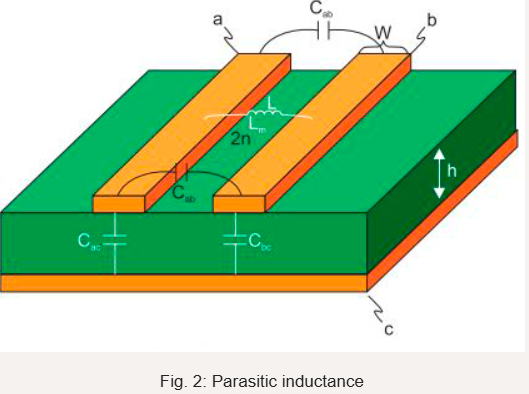
- Place the conductors at right angles to each other. This will reduce crosstalk due to parasitic inductance.
- Place the largest and most important components first.
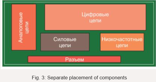
- Place analog and digital components on separate areas of the board.
- Avoid placing tall components (such as electrolytic capacitors) next to shorter ones, as this may negatively affect the quality of the solder joints.
- Powerful components should be placed as far away from other components as possible to optimize heat dissipation on the board.
Pinout to prevent interference
Incorrect pin placement can affect electromagnetic coupling and cause mutual inductance. Following the recommendations below will improve the efficiency of component pin placement on the PCB:
- Avoid placing pins close to each other.
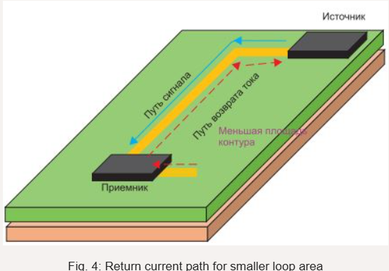
- Design the return path close to the main current path in a low-noise area. This will help reduce the current loop area.
- To increase the reliability of the board, it is necessary to perform complex grounding under the contacts.
Signal routing in automotive printed circuit boards
Use two to four vias per layer to connect layers carrying high currents. This will increase reliability, reduce resistive and inductive losses, and improve thermal conductivity. When routing signals, adhere to the following guidelines:
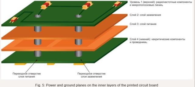
- Use internal power and ground layers.
- Protect sensitive signals from noise sources with shielding layers and provide controlled impedance
- for their transmission. Conductive tracks on the board should be as short and straight as possible.
- It is desirable that the tracks on two-layer printed circuit boards are located horizontally on one side and vertically on the other.
- Onmultilayer boards, alternate vertical and horizontal trace routing on adjacent layers.
Effective temperature management
When using components that absorb more than 10 mW or conduct more than 10 mA, special attention must be paid to thermal management to ensure effective heat dissipation on the board. Here are some recommendations to help you achieve this goal:
- Choose the correct copper layer thickness and use signal holes as heat sinks to increase thermal conductivity.
- Place signal vias close to surface-mount components or directly below SMD components.
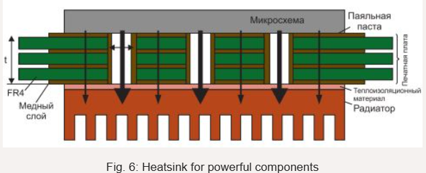
- For powerful components, use heatsinks.
- Place metal thermal pads under the parts of the board that will be exposed to heat.
- To transfer heat from thermal pads to ground planes, vias filled with heat-conducting material can be used.
- Use metal cores and polyimide materials as they have improved thermal properties.
- Use multiple ground and power planes and connect them directly to heat sources via thermal vias. This will help reduce operating temperatures and improve thermal performance across the board.
- Prefer materials with a high Tg (glass transition temperature) to ensure the board can withstand high ambient temperatures.
PCB design analysis
Don’t neglect analyzing the project for any errors that may have been made during development or adjustments. This checklist will help you conduct a thorough review:
- Assess how correctly the distance between components on the printed circuit board as a whole and on its individual layers is calculated.
- Check the clearance between the power and ground wires. Ensure there is sufficient clearance on the board for the ground lines.
- Check that the analog and digital circuits are properly grounded.
- Remove any unwanted lines such as open caps etc. if found.
- Check that all connections on the board match the connections in the circuit diagram.
- Ensure that the outer edge of the power plane is sufficiently spaced from the edge of the PCB. This will prevent short circuits when it extends to the edge.
- Assess signal integrity, power integrity, EMI, and check the overall safety of the PCB.
Standards governing the design process of automotive printed circuit boards
Printed circuit boards (PCBs) are complex, multi-component electronic devices whose reliability determines the efficient operation of many automotive systems, including communications, safety, driver assistance systems, engine control units, and others. Rapid technological advancements in the automotive industry, particularly in the field of autonomous vehicles, are leading to ever-increasing complexity in electronic circuits. This, in turn, requires the designer to understand and adhere to the standards that govern the automotive PCB design process, namely IATF 16949, IPC-6012 Class 3, AEC-Q100, and SAE J3016_201401.
The IPC-6012 standard describes requirements for the conductive pattern, solder mask thickness, copper layers, and other parameters that must be considered during the design and manufacture of automotive circuit boards. Here are some recommendations based on the information in IPC-6012:
Make sure that the hole positioning accuracy is within the established tolerance, which is
100 µm.
Maintain the minimum AR (diameter-to-depth ratio) for through holes. When drilling mechanically, use the smallest drill bit available.
Make sure that the distance between the hole walls does not exceed 40% of the dielectric thickness.
Before applying solder mask, check the board surface for cleanliness. The acceptable contamination level is 0.75 g/cm2 sodium chloride equivalent.
Before assessing the board for bending and twisting after the soldering process, it is necessary to ensure that there are no defects such as cracks, breaks, and short circuits.
Ensure that solder mask parameters comply with IPC-6012DA. For example, if you are using a board with Class 3 copper plating and a base copper thickness of 18 µm, the acceptable solder mask thickness is calculated based on Table 1.
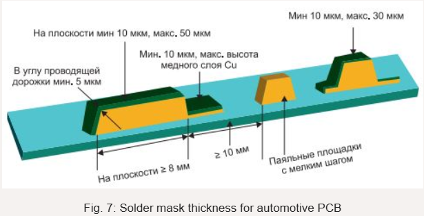
Table 1
| Region | Solder mask thickness |
| Conductor located near surface mount pads | Minimum 5 microns
Maximum 30 microns |
| Grounding layers | Minimum 10 microns
Maximum 60 microns |
Automotive circuit boards must be highly reliable and have a long service life, so IPC Class 3 printed circuit boards are the best choice for this application. Below are some design tips for such boards:
Plated holes should be 0.4 mm larger than the pin diameter. The required hole fill for through-hole pins is 75%.
The minimum internal contact belt must not be less than 0.02 mm, and the external one must not be less than 0.04 mm.
Adhere to the specified tolerances for the conductive pattern. The permissible deviation for boards up to 300 mm in size is ±75 µm, up to 450 mm in size is ±112 µm, and up to 600 mm in size is ±150 µm (Table 2).
Table 2
| Hole | Contact pad | Platform with remote metallization | PCB thickness | Aspect ratio |
| 0.008″ | 0.023″ | 0.033″ | Up to 0.062″ | 7.75:1 |
| 0.010″ | 0.025″ | 0.035″ | Up to 0.100″ | 10:01 |
| 0.012″ | 0.027″ | 0.037″ | Up to 0.120″ | 10:01 |
| 0.0135″ | 0.028″ | 0.038″ | Up to 0.135″ | 10:01 |
Grounding of through-hole mounting
Mounting holes must be plated and grounded. One problem is the poor impedance characteristics of
various circuits. This is primarily caused by the use of various electronic components and their connection methods. Therefore, the following practical recommendations can be used when designing automotive electronics:
- In sensitive areas, place inductive modules near through holes.
- Apply appropriate filtering schemes depending on the through-hole configuration.
- Use thin copper layers. This will reduce the effects of parasitic inductance in through-holes.
Optimization of high-frequency circuit
Printed circuit board design for automotive applications ideally integrates high-frequency (RF) circuitry. Addressing issues related to compatibility, power consumption, and long-term reliability can be challenging. Consider the following guidelines during the design process:
- Use high-linearity active or interface devices.
- Consider the RF interface efficiency, current consumption, and power dissipation.
- Select a high performance RF filter to minimize insertion loss, temperature drift, and interference.
- Use components that combine transmit, receive, and filter functions in a single device.
Use proper grounding techniques
In the process of designing grounding in an automotive device:
- Provide a single ground connection point on each board.
- Provide a large ground plane with the lowest possible resistance.
- Connect ground to the input circuit using a through-hole matrix.
- Always connect the wire shields to ground.
Preventing electromagnetic interference
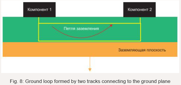
It’s vital to include measures to prevent electromagnetic interference in any electrical circuit. This is essential to ensure the reliable operation of the vehicle as a whole. You can protect your device from interference using the following methods:
- The area of any closed loop must be minimal.
- Provide shielding for the device and components that generate interference.
- Use differential pairs to transmit signals on the board.
- Optimizing trace routing and component pin assignments helps reduce signal interference.
- Increase the capacity of power supply filters, use RC decoupling circuits.
- Use ignition systems without a distributor to eliminate the source of interference and electromagnetic radiation.
- Using a CAN bus reduces the number of wires required, thus reducing the impact of electrical interference and eliminating electromagnetic compatibility issues.
Types of automotive printed circuit boards
Various types of printed circuit boards (PCBs) are used in automotive electronics. The appropriate type is selected based on the functional requirements and the space constraints of the device’s design.
Rigid boards: Made of hard laminates such as FR4, Rogers, etc. and used in monitors and rear view cameras.
Flexible circuit boards : These have a flexible backing for mounting electronic components. They can be bent and twisted, making them suitable for use in confined spaces. These boards are used in stereo and monitoring systems.
Rigid-flex boards : These boards combine both technologies in a single design. They are used in lighting systems.
LED printed circuit boards : Modern cars require circuits capable of efficiently dissipating large amounts of heat to power powerful and bright LEDs. These are called metal-core circuit boards (MCPCBs). They are used in brake systems, headlights, and turn signals.
Heavy-duty copper printed circuit boards (PCBs) : These boards use copper foil 100 microns thick or more for the outer and inner layers. They are used in vehicle security and alarm systems.
Depending on the intended application, multilayer, double-sided, or single-sided printed circuit boards may also be used. Modern cars are equipped with complex, high-tech electronic devices, including printed circuit boards responsible for engine management, fuel efficiency, autopilot system control, and much more. An automotive circuit board must meet all requirements related to functionality, thermal management, and signal integrity. The recommendations provided in this article will certainly help the designer create a reliable automotive printed circuit board.
